
Ever wondered what happens inside the IOActive silicon lab? For the next few weeks we’ll be posting a series of blogs that highlight some of the equipment, tools, attacks, and all around interesting stuff that we do there. We’ll start off with Andrew Zonenberg explaining the basics of CMOS layout.
Basics of CMOS Layout
When describing layout, this series will use a simplified variant of Mead & Conway’s color scheme, which hides some of the complexity required for manufacturing.
|
Material
|
Color
|
|
P doping
|
|
|
N doping
|
|
|
Polysilicon
|
|
|
Via
|
|
|
Metal 1
|
|
|
Metal 2
|
|
|
Metal 3
|
|
|
Metal 4
|
|
The basic building block of a modern integrated circuit (IC) is the metal-oxide-semiconductor field effect transistor, or MOSFET. As the name implies, it is a field-effecttransistor (an electronic switch which is turned on or off by an electric field, rather than by current flow) made out of a metal-oxide-semiconductor “sandwich”.
(Terminology note: In modern processes, the gate is often made of polycrystalline silicon, aka polysilicon, rather than a metal. As is the tradition in the IC fab literature, we typically use the term “poly” to refer to the gate material, regardless of whether it is actually metal or poly.)
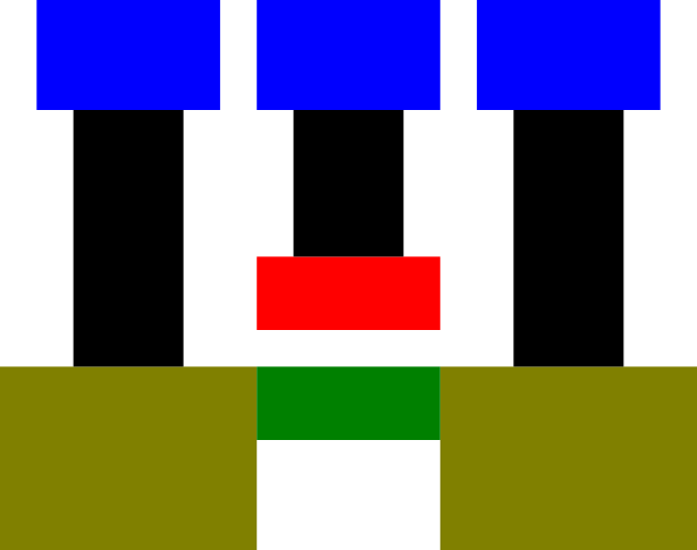
Without further ado, here’s a schematic cross-section and top view of an N-channelMOSFET. The left and right terminals are the source and drain and the center is the gate.
Figure 1: N-channel MOFSET
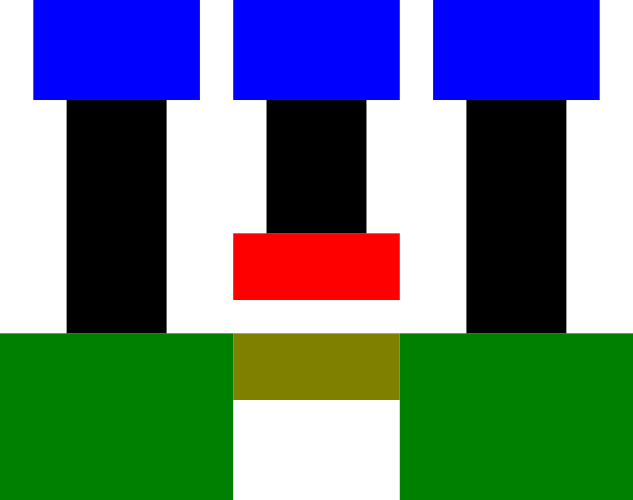
Cross-section view
Top view
Signals enter and exit through the metal wires on the top layer (blue, seen head-on in this view), and are connected to the actual transistor by vertical connections, or vias (black). The actual transistor consists of portions of a silicon wafer which have been “doped” with various materials to have either a surplus (N-type, green) or lack (P-type, yellow) of free electrons in the outer shell. Both the source and drain have the same type of doping and the channel between them has the opposite type. The gate terminal, made of poly (red) is placed in close proximity to the channel, separated by a thin layer of an insulator, usually silicon dioxide (usually abbreviated simply as “oxide,” not shown in this drawing).
When the gate is held at a low voltage relative to the bulk silicon (typically circuit ground), the free electrons near the channel in the source and drain migrate to the channel and fill in the empty spots in the outer electron shells, forming a highly non-conductive “depletion region.” This results in the source and drain becoming electrically isolated from each other. The transistor is off.
When the gate is raised to a high voltage (typically 0.8 to 3.3 volts for modern ICs), the positive field pulls additional electrons up into the channel, resulting in an excess of charge carriers and a conductive channel. The transistor is on.
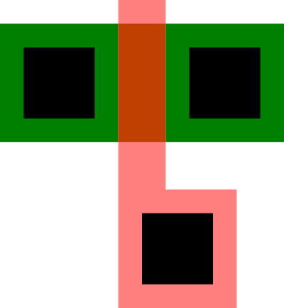
Meanwhile, the P-channel MOSFET, shown below, has almost the same structure but with everything mirrored. The source and drain are P-doped, the channel is N-doped, and the transistor turns on when the gate is at a negativevoltage relative to the bulk silicon (typically the positive power rail).
Figure 2: P-channel MOFSET
Cross-section view
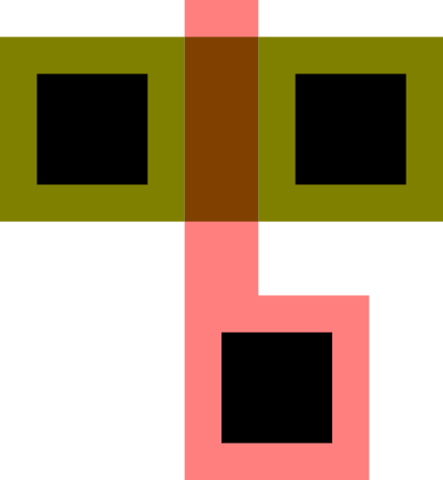
Top view
Several schematic symbols are commonly used for MOSFETs. We’ll use the CMOS-style symbols (with an inverter bubble on the gate to denote a P-channel device and no distinction between source and drain). This reflects the common use of these transistors for digital logic: an NMOS (at left below) turns on when the gate is high and a PMOS (at right below) when the gate is low. Although there are often subtle differences between source and drain in the manufacturing process, we as reverse engineers don’t care about the details of the physics or manufacturing. We just want to know what the circuit does.
Figure 3: Schematic symbols
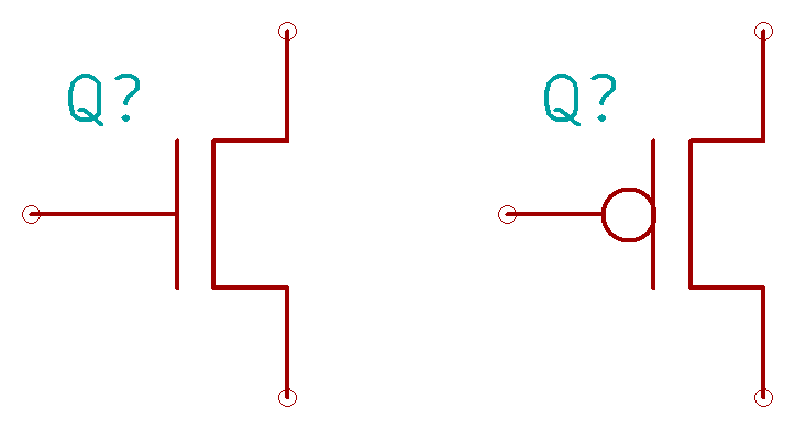
NMOS PMOS
So, in order to reverse engineer a CMOS layout to schematic, all we need is a couple of photographs showing the connections between transistors… right? Not so fast. We must be able to tell PMOS from NMOS without the benefit of color coding.
As seen in the actual electron microscope photo below (a single 2-input gate from a Xilinx XC2C32A, 180nm technology), there’s no obvious difference in appearance.
Figure 4: Electron microscope view of a single 2-input gate
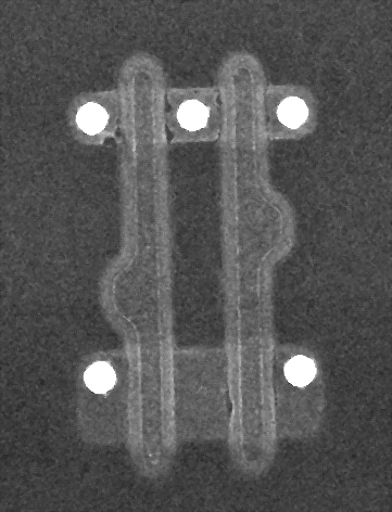
We can see four transistors (two at the top and two at the bottom) driven by two inputs (the vertical poly gates). The source and drain vias are clearly visible as bright white dots; the connections to the gates were removed by etching off the upper levels of the chip but we can still see the rounded “humps” on the poly where they were located. The lack of a via at the bottom center suggests that the lower two transistors are connected in series, while the upper ones are most likely connected in parallel since the middle terminal is broken out.
There are a couple of ways we can figure out which is which. Since N-channel devices typically connect the source to circuit ground and P-channel usually connect the source to power, we can follow the wiring out to the power/ground pins and figure things out that way. But what if you’re thrown into the middle of a massive device and don’t want to go all the way to the pins? Physics to the rescue!
As it turns out, P-channel devices are less efficient than N-channel – in other words, given two otherwise identical transistors made on the same process, the P-channel device will only conduct current about 30-50% as well as the N-channel device. This is a problem for circuit designers since it means that pulling an output signal high takes 2-3 times as long as pulling it low! In order to compensate for this effect, they will usually make the P-channel device about twice as wide, effectively connecting two identical transistors in parallel to provide double the drive current.
This leads to a natural rule of thumb for the reverse engineer. Except in unusual cases (some I/O buffers, specialized analog circuitry, etc.) it is typically desirable to have equal pull-up and pull-down force on a signal. As a result, we can conclude with fairly high certainty that if some transistors in a given gate are double the width of others, the wider ones are P-channel and the narrower are N-channel. In the case of the gate shown above, this would mean that at the top we have two N-channel transistors in parallel and at the bottom two P-channel in series.
Since this gate was taken from the middle of a standard-cell CMOS logic array and looks like a simple 2-input function, it’s reasonable to guess that the sources are tied to power and drains are tied to the circuit output. Assuming this is the case, we can sketch the following circuit.
Figure 5: CMOS 2-input circuit
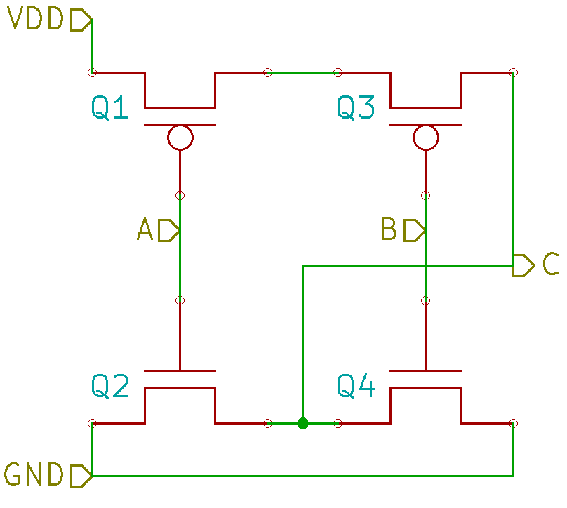
This is a textbook example of a CMOS 2-input NOR gate. When either A or B is high, either Q2 or Q4 will turn on, pulling C low. When both A and B are low, both Q1 and Q3 will turn on, pulling C high.
Stay tuned for the next post in this series!