Good Afternoon Internet,
Chris Valasek here. You may remember me from such automated information kiosks as “Welcome to Springfield Airport”, and “Where’s Nordstrom?” Ever since Dr. Charlie Miller and I began our car hacking adventures, we’ve been asked about the upcoming Vehicle-to-Vehicle (V2V) initiative and haven’t had much to say because we only knew about the technology in the abstract.
I finally decided to read the proposed documentation from the National Highway Traffic Safety Administration (NHTSA) titled: “Vehicle-to-Vehicle Communications: Readiness of V2V Technology for Application” (https://www.ioactive.com/wp-content/uploads/2014/09/Readiness-of-V2V-Technology-for-Application-812014.pdf). This is my distillation of a very small portion of the 327-page document.
While there are countless pages of information regarding cost, crash statistics, consumer acceptance, policy, legal liability, and fuel economy, as a breaker of things, I was most interested in any technical information I could extract. In this blog post, I list some interesting bits I stumbled upon when reading the document. I skipped over huge portions I felt weren’t applicable to my investigation. Mainly anything that didn’t have to do with a purely technical implementation. In addition, any diagrams or pictures in this blog post were taken directly from “Vehicle-to-Vehicle Communications: Readiness of V2V Technology for Application”.
A Very Brief History
Although currently a hot topic in the automotive world, the planning, design, and testing of the V2V infrastructure started over 11 years ago. It has gone from special purpose lanes in San Diego to a wireless infrastructure designed to be transparent to the end user. For those not in the know, a pilot program was deployed in Ann Arbor, MI from August 2012 to February 2014. This isn’t a harebrained scheme to a long-standing problem, but has been thought about and fine-tuned for quite some time.
Overview
The V2V system is designed (obviously) to reduce death, injuries, and economic loss from motor vehicle crashes. Many people, including me, didn’t realize this initial proposal is only designed to provide visual and audible warnings to the driver and DOES NOT include or plan for physical alterations of the automobile based on V2V communications. For example, the V2V system will not brake a car in the event of an impending accident, but only warn the driver to apply the brake (although V2V could be used by current in-car systems, such as Collision Avoidance, to augment their functionality).
The main components:
Forward Collision Warning (FCW) – Warns you if you’re about to smash into something in front of you.
Emergency Electronic Brake Lights – Warns you when the person in front of you is slowing down while you’re reading your Twitter feed.
Do Not Pass Warning – Really for unintentional drift more than you trying to push the limit to pass that big rig on the left side of the dotted line.
Left Turn Assist (LTA) — Warns you if there is a car coming when making a left turn.
Intersection Movement Assist (IMA) – Figuring out how not to smash into several different cars at a 4-way intersection is hard, let’s go shopping!
Blind Spot Warning + Lane Change Warning – Warns you if you’re about to smash into something while changing lanes. No more “Rubbin is racin” I guess.
This picture gives you a better idea of some of the scenarios mentioned above.
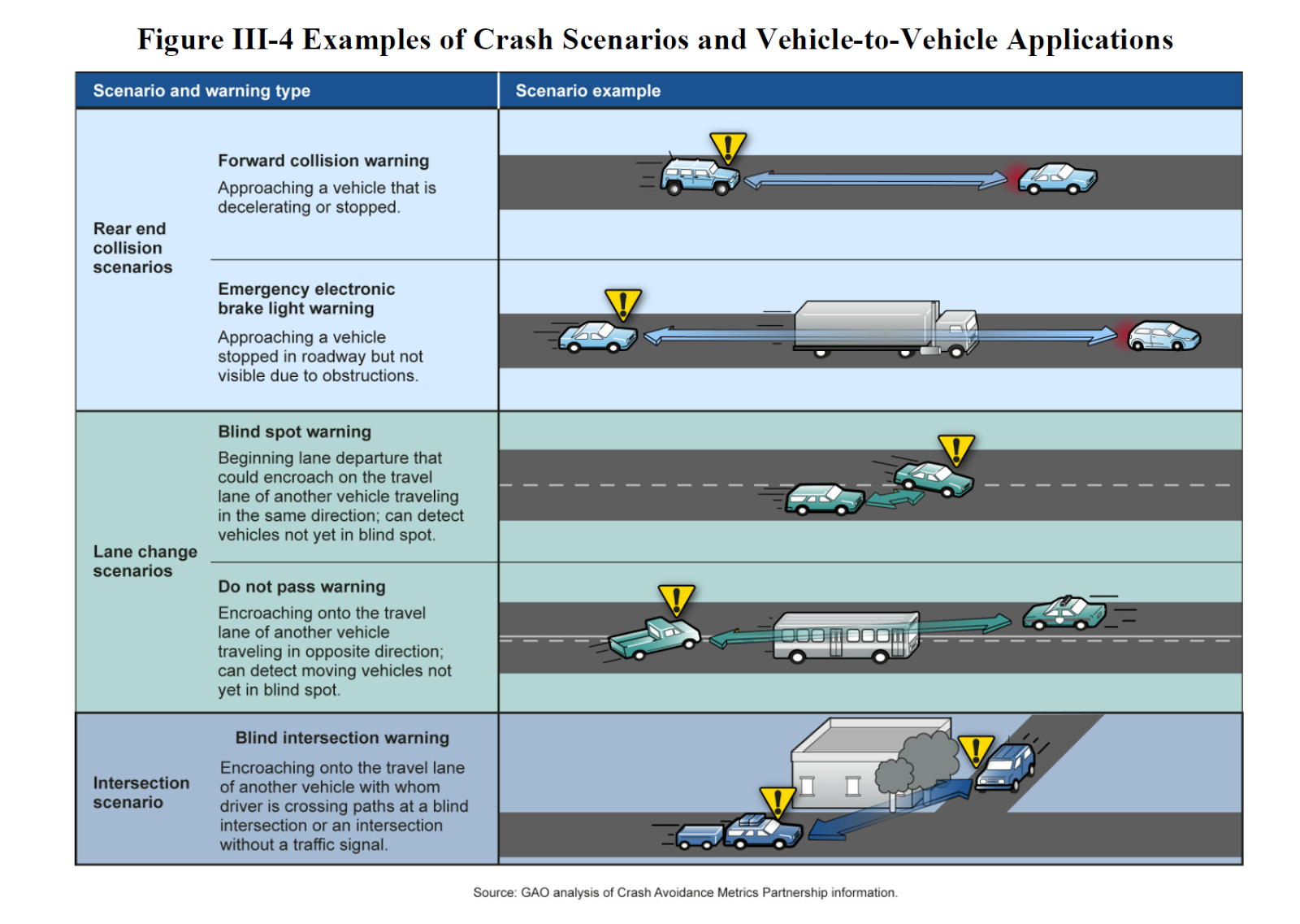
You’ll notice that none of the safety mechanisms mentioned earlier involve performing any physical actions on the automobile. The designers of the V2V system realize that false positives could be a huge problem with warnings. Just imagine how scared people would be if their automobile braked or steered without cause in an attempt to protect them.
Notable Items:
- The document predicts it will take 37 years for V2V to penetrate an entire fleet.
- Rear and Forward Collision Warnings appear to be capable of saving the most money.
- NHSTA does not expect an immediate difference, due to lack of adoption, but hopes to gain ground as time goes on.
My Thoughts
All these features seem like they will greatly increase vehicle and passenger safety. My one concern is a whole V2V infrastructure is being developed without much thought given to the physical control of a vehicle. It seems like the next logical step is to not only warn drivers if they are about to collide, but to prevent it. Maybe this will always be left up to the manufacturer, maybe not.
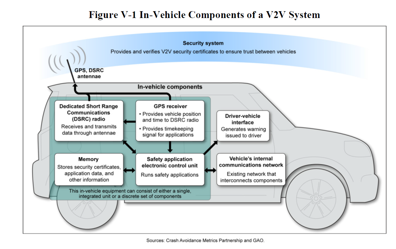
Components/Terms
On Board Equipment (OBE) – The device in your car that will communicate with the V2V infrastructure. It will either be OEM (put there by the manufacturer) or aftermarket (sold separately from the car, mobile phone, standalone device, and so on).
Road Side Equipment (RSE) – These devices will connect to the vehicles around them. They can be on road curves that warn the car about its speed, traffic lights, stop signs, and so on.
Dedicated Short-range Communications (DSRC) – The short-range wireless communications that RSE and OBE use to communicate.
Driver Vehicle Interface (DVI) – This interface will display the V2V warnings.
Basic Safety Message (BSM) – This is a message sent to and received from other OBE and RSE devices to make the V2V system work. For example, it could announce the current speed of the vehicle.
Security Credentials Management System (SCMS) – The systems that manage all of the credentials for V2V systems, such as the certificates used to authenticate BSMs.
Communications
The most interesting portion of the document for me was the technical information about the underlying communications system. I think many people want to understand what kind of wireless communications will be implemented for the vehicles and devices with which they will interact.
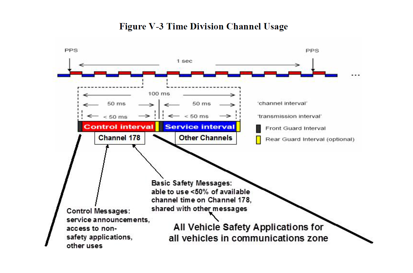
The V2V infrastructure will operate on the 5.8 – 5.9 GHz band (5850 – 5925 MHz) using seven (7) non-overlapping 10 MHz channels, with a 5 MHz guard band at the beginning of each frequency range. Channel 172 will be used to send public safety information.
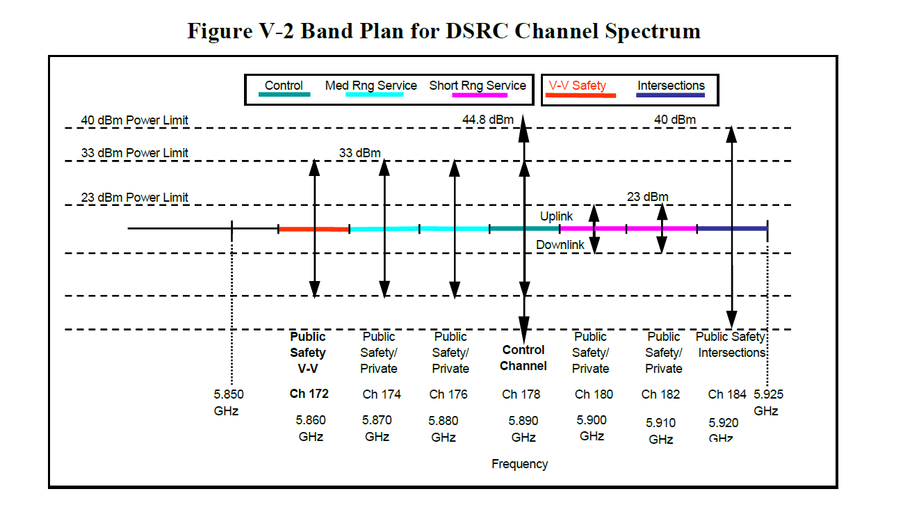
Since these devices, much like your AM/FM radio, can only be on one channel at a time, switching is necessary. Switching between the Control Channel (CCH) and Service Channel (SCH) occurs every 50 ms to transmit or receive DSRC messages emitted by other vehicles or RSE. There is a 4 ms front guard leaving only 46 percent of “potentially” available bandwidth for BSM transmissions.
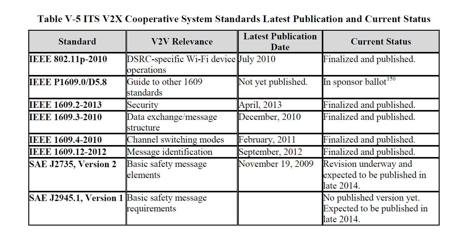
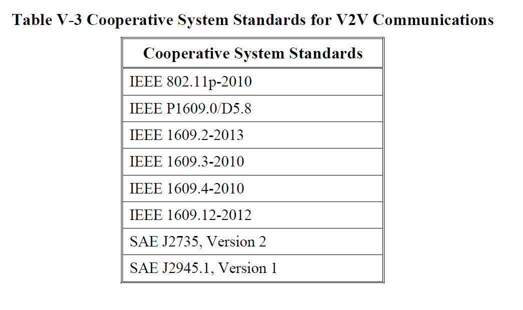
DSRC messages will be broadcast (omnidirectional for up to 300 meters) on a standardized network (IEEE 1609.4) over a standardized wireless layer IEEE 802.11p. The chart below shows all of the system standards currently anticipated for the first generation V2V system.
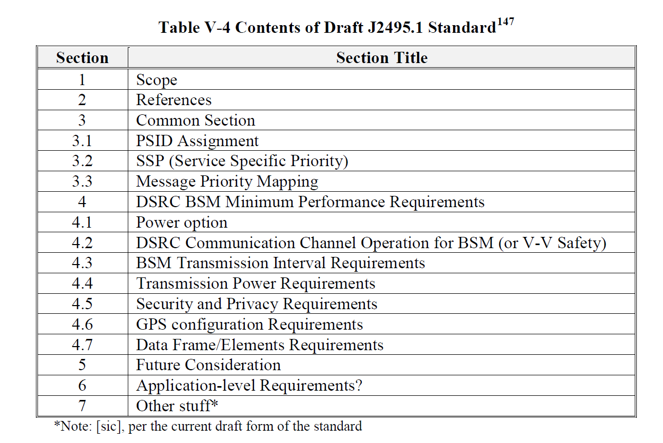
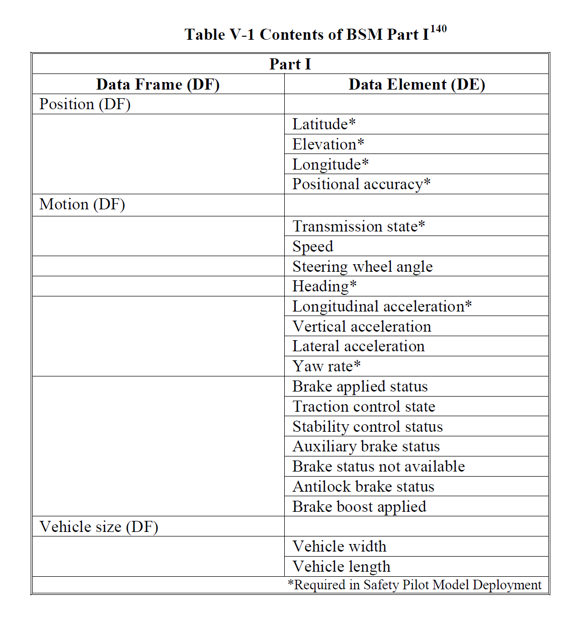
BSM messages also have a certain format, which is partially listed below. Please see the original document for more detailed information. Each message should have a packet size of 200 – 500 bytes with a maximum required range of 50 – 300 meters.
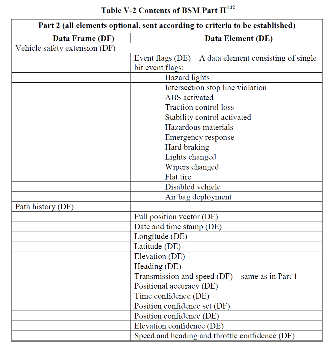
Note: This is a partial snippet of the BSM Part II contents.
One main take away was that BSM messages are NOT encrypted; therefore, they could be viewed over the air by interested parties. The messages are, however, authenticated via a signing mechanism (discussed in the next section).
Notable Items:
NHSTA is unsure if current WiFi infrastructure will interfere with the communications based on the devices. The claim is that more research is required.
NHSTA claims the system will NOT collect or store any data identifying individuals or individual vehicles, nor will it create the ability for the government to do so.
NHSTA claims it would be extremely difficult for third parties to use the system to track a vehicle.
“NHTSA is aware of concerns that the V2V system could broadcast or store BSM data (such as GPS or path history) that, if captured by a third party, might facilitate very-localized vehicle tracking. In fact, the broadcast of unencrypted GPS, path history, and other data characteristics in or derived from the BSM appears to introduce only very limited potential risks to individual privacy.”
“It is theoretically possible that a third party could try to capture the transitory locational data in order to track a specific vehicle. However, we do not see a scenario in which one wishing to track a vehicle would choose the V2V system as the means.”
“To date, NHTSA’s V2V research has not included research specific to this issue, as researchers assumed that the possibility of cyber-attacks on motor vehicles was an existing vector of risk – not a new one created by V2V technologies.”
My Thoughts:
This is an amazingly complex system that is going to send, receive, and analyze data in real-time.
It will be interesting to see if people figure out how to use BSM messages to track vehicles or enumerate personal information due to their lack of encryption.
It looks like you could use BSM messages to gather information and track a vehicle, but I’m unsure of the practicality of doing so.
I don’t really know enough about radio/wireless to comment much more, but I’d love to hear other people’s thoughts.
Security
The V2V system, while sending a majority of the information in cleartext, does have mechanisms that are designed for security. After much internal debate, it was decided that a Public Key Infrastructure (PKI) would be implemented to prove authenticity when sending and receiving messages. I think we’re all familiar with the PKI system, since we use it every day on the Internet to do our banking, chatting, and general internetting. Because this is a blog post, I only sampled a small set of the information available in the document. Also, I’m far from a crypto expert and will do my best to briefly explain the system that is being implemented. Please excuse or correct any errors you see with a quick tweet to @nudehaberdasher.
As stated before, BSMs are NOT encrypted, but verified with a digital signature, meaning that each message must be signed before it is sent and checked upon receipt. This trust system is a requirement, since thousands of messages will be authenticated in real-time when driving a vehicle that uses the V2V system.
Like our Internet PKI system, there is a Certificate Authority (CA) but, to quote the paper:
“We note that the interactions between the components shown in Figure <not-shown> are all based on machine-to-machine performance. No human judgment is involved in creation, granting, or revocation of the digital certificates.”
This means that there will not be human involvement when putting new devices on the V2V system.
A simplified version of the system can be seen below.
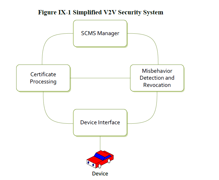
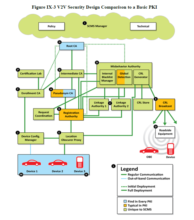
Obviously, the system is much more complex, involving preinstalled certificates, which are supposed to last five minutes each, a signing authority, and even a misbehavior authority responsible for revoking certificates for a variety of reasons. A comparison between the V2V PKI system and the PKI system we currently use on the Internet is illustrated below.
“Initial deployment is assumed to last for three years, and requires that OBEs on newly manufactured vehicles download a three-year batch of certificates. These batches would include reusable, overlapping five-minute certificates valid for one week. The term “overlapping” in this context refers to the fact that any certificate can be used at any time during the validity period. The batches would be good for one week and at this point are assumed to be around 20 certificates per week, which equates to 1,040 for one year of certificates. As the frequency of the certificate download batch changes for full deployment, the number and therefore size of the certificate batches also changes accordingly.”
It looks as if there are two options for preinstalled certificates, which will be placed there by OEMs and aftermarket solution providers:
Option 1: Three-year reusable, non-overlapping five-minute certificates
Option 2: Three-year batches of reusable, overlapping, 260 five-minute certificates valid for one week
Certificates will be managed by the SCMS and communications with devices will go as follows:
- UPLOAD – a request for new certificates
- DOWNLOAD – new certificates
- UPLOAD – a misbehavior report
- DOWNLOAD – a full/partial CRL
- Conduct other data functions or system updates
Certificate renewal, updates, and revocation still seem to be up in the air. Certificate downloads could happen through cellular, WiFi, or DSRC. The most likely scenario will be DSRC due to cost and availability issues. New certificates could be updated in-full on a daily basis, or the system could use incremental updates to save time and bandwidth.
While the design of the system seems to be pretty well developed, the details of the implementation and ownership still seem to be undecided. It looks like only time will tell who will own and administer this system and in what fashion it will be administered.
Notable Items:
“As no decisions about ownership or operation have been made, we do not advocate for public or private ownership, but include the basic functions we expect the SCMS Manager would perform in our discussions and analyses.”
“Most SCMS functions listed above are fairly well developed. One critical function, which has not yet been fleshed out adequately for DOT to assess, is the Misbehavior Authority (MA) — the central function responsible for processing misbehavior reports generated by OBE and producing and publishing the CRL.”
“Global detection processes have not yet been defined.”
Research into the PKI system will continue into 2016.
“Publication of the seed is sufficient to revoke all certificates belonging to the revoked device, but without the seed an eavesdropper cannot tell which certificates belong to a particular device. (Note: the revocation process is designed such that it does not give up backward privacy.)”
Internal Blacklist – This would be used by the SCMS to make sure that an OBE asking for new certificates is not on the revoked list. If a vehicle or device is on the list, no certificate updates will be issued.
My Thoughts:
Be it that devices with valid certificates and valid certificate updates will be the hands of an ‘attacker’, I’m interested to see how well the certificate revocation functionality works.
Without any decision on certificate revocation, will it be implemented? If so, will it be done correctly and robustly?
How fast can certificates be revoked?
Sending spoofed, legitimately signed messages for even five minutes at a busy intersection could cause a massive disruption.
Private keys are going to be in infrastructure devices, meaning there’s a good chance they won’t be ‘private’ for long.
Crypto people do your crypto thing on this.
Conclusion
I think the V2V technology is very interesting but still has many questions to answer, due to its massive technical complexity and huge economic cost. Additionally, I don’t think people have much to be worried about in the first iteration since there are only audible and visual warnings to the driver, without any direct effect on the vehicle.
I hope that, when developing these systems, planning and design would be considered around vehicle control and not only warnings, as it seems like true V2V accident avoidance is the next logical step. Additionally, there is probably a good chance that current vehicle bus infrastructure is used to provide warnings to the driver, which means there is yet another remote entry point to the vehicle which potentially uses the vehicle’s network for communication. From an attacker’s perspective, all remote communication systems that interact with the car will be seen as attack surfaces.
My last thought is that a true V2V infrastructure is further away than many people think. While we may have fringe devices in the coming years, full fleet adoption isn’t expected until 2037, so we can all go back to worrying about our robot overlords taking over in 2029.
Chris Valasek @nudehaberdasher
Special Thanks: Charlie Miller (@0xcharlie) and Zach Lanier (@quine)