What is an FPGA?
Field-Programmable Gate Arrays (FPGAs) are a type of Integrated Circuit (IC) that can be programmed or reprogrammed after manufacturing. They consist of an array of logic blocks and interconnects that can be configured to perform various digital functions. FPGAs are commonly used in applications where flexibility, speed, and parallel processing capabilities are required, such as telecommunications, automotive, aerospace, and industrial sectors.
FPGAs are often found in products that are low volume or demand short turnaround time because they can be purchased off the shelf and programmed as needed without the setup and manufacturing costs and long lead times associated with Application-Specific Integrated Circuits (ASICs). FPGAs are also popular for military and aerospace applications due to the long lifespan of such hardware as compared to typical consumer electronics. The ability to update deployed systems to meet new mission requirements or implement new cryptographic algorithms—without replacing expensive hardware—is valuable.
These benefits come at a cost, however: additional hardware is required to enable reprogramming. An FPGA-based design will use many more transistors than the same design implemented as an ASIC, increasing power consumption and per-device costs.
Implementing a circuit with an FPGA vs an ASIC can also come with security concerns. FPGA designs are compiled to a “bitstream,” a digital representation of the circuit netlist, which must be loaded into the FPGA for it to function. While bitstream formats are generally undocumented by the manufacturer, several projects are working towards open-source toolchains (e.g., Project X-Ray for the Xilinx 7 series) and have reverse engineered the bitstream formats for various devices.
FPGA bitstreams can be loaded in many ways, depending on the FPGA family and application requirements:
- Serial or parallel interfaces from an external processor
- JTAG from a debug cable attached to a PC
- Serial or parallel interfaces to an external flash memory
- Separate stacked-die flash memory within the same package as the FPGA
- Flash or One-Time-Programmable (OTP) memory integrated into the FPGA silicon itself
In this post, we will focus on Xilinx because it was the first company to make a commercially viable FPGA back in 1985 and continues to be a world leader in the field. AMD acquired Xilinx in 2020 in a deal worth $60 billion, and today they control over 50% of the world’s programmable logic chips.
The Spartan™ 6 family of Xilinx FPGAs offers low-cost and low-power solutions for high-volume applications like displays, military/emergency/civil telecommunications equipment, and wireless routers. Spartan 6 was released in 2009, so these chips are relatively low-tech compared with their successors, the Spartan 7 and Xilinx’s higher end solutions (e.g., the Zynq and Versal families).
The Spartan 6 bitstream format is not publicly known, but IOActive is aware of at least one research group with unreleased tooling for it. These devices do not contain internal memory, so the bitstream must be provided on external pins each time power is applied and is thus accessible for an attacker to intercept and potentially reverse engineer.
FPGA vendors are, of course, aware of this risk and provide security features, such as allowing bitstreams to be encrypted on external flash and decrypted on the FPGA. In the case of the Spartan 6 family, the bitstream can be encrypted with AES-256 in CBC mode. The key can be stored in either OTP eFuses or battery-backed Static Random Access Memory (SRAM), which enables a self-destruct function where the FPGA can erase the key if it detects tampering.
The AES block used in the Spartan 6, however, is vulnerable to power analysis, and a team of German researchers developed a successful attack against it: “On the Portability of Side-Channel Attacks – An Analysis of the Xilinx Virtex 4, Virtex 5, and Spartan 6 Bitstream Encryption Mechanism.”
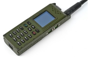
An example of a Xilinx Spartan 6 application is the Russian military radio R-187-P1 made by Angstrem, so we decided to use this as our test case.
AZART R-187-P1 Product Overview
Since its release in 2012, several researchers have discovered that the radio provides built-in protocols to allow communication across multiple standards, including older analogue Russian radios, UAV commands, and even TETRA. While the advertised frequency range is 27 to 520 MHz, recent firmware updates enabled a lower range of frequencies down to 100 kHz with AM.
The features of this radio are fairly well known. The following was posted by @SomeGumul, a Polish researcher, on Twitter/X:
The trophy in the form of the Russian radio station “Azart”, announced by the Russians as a “native, Russian” sixth-generation device for conducting encrypted conversations, works on American radio components. The basis of the encryption system is, in particular, the Spartan®-6 FPGA (field-programmable gate array) system. It is produced by the American company XILINX (AMD) in Taiwan.
Ironically, despite being advertised as the forefront of Russia’s military technical prowess, the heart of this device was revealed by Ukrainian serviceman Serhii Flash (Сергей Флэш) to be powered by the Spartan 6 FPGA. This FPGA is what enables the handheld radio’s capabilities to be redefined by mere software updates, allowing its users to speak over virtually any radio standard required—past, present, or future. While most of the currently implemented protocols are unencrypted to allow backward compatibility with other older, active service equipment, communication between two AZART radios enables frequency hopping up to 20,000 frequencies per second. This high rate of frequency hopping creates challenges for eavesdropping and position triangulation. The radio’s implementation of TETRA also supports encryption with the inclusion of a supporting radio trunk, where the radio is referred to as being in Trunked Mode Operation (TMO). Otherwise, while in Direct Mode Operation (DMO), the radio only supports voice scrambling in the time and frequency domains.
20,000 frequency hops per second is quite a feat for a radio. Extremely precise timing is required for two or more radios to sync across hops and still communicate clearly. This timing source is gained wirelessly from GPS and GLONASS. As such, this advanced feature can be disabled simply by jamming GPS frequencies.
While this attack may be sufficient, GPS signals are ubiquitous and neutral sources of precise timing that are often required by both sides of any conflict. So, while jamming the frequencies may work in a pinch, it would be cleaner to find a solution to track this high rate of frequency hopping without having to jam a useful signal. To find this solution, we must investigate the proprietary Angstrem algorithm that drives the pseudo-random frequency hopping. To do this, we begin by looking at the likely driver: the Spartan 6 FPGA.
Chipset Overview
It is currently unknown if the Spartan 6 on the AZART is utilizing an encrypted bitstream; however, due to its wartime purpose, it must not be ruled out. While waiting for the procurement of a functioning radio, IOActive began a preliminary investigation into the functioning of the Spartan 6 with a specific focus on areas related to encryption and decryption of the bitstream.
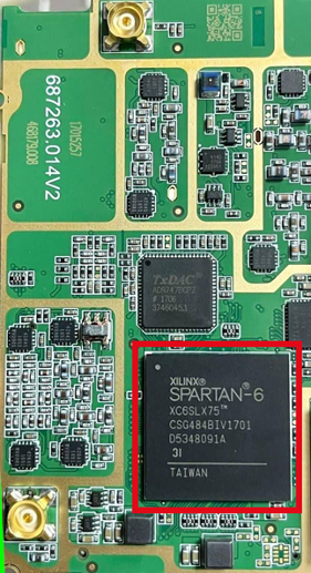
At the time of writing this post, the XC6SLX75-3CSG484I sells for around $227 from authorized US distributors; however, it can be obtained for much lower prices in Asian markets, with sellers on AliExpress listing them for as low as $8.47. While counterfeits are prevalent in these supply chains, legitimate parts are not difficult to obtain with a bit of luck.
In addition to the FPGA, one other notable component visible on the board is the Analog Devices TxDAC AD9747, a dual 16-bit 250 Msps Digital-to-Analog Converter (DAC) intended for SDR transmitters. Assuming this is being used to transmit I/Q waveforms, we can conclude that the theoretical maximum instantaneous bandwidth of the radio is 250 MHz, with the actual bandwidth likely being closer to 200 MHz to minimize aliasing artifacts.
Device Analysis
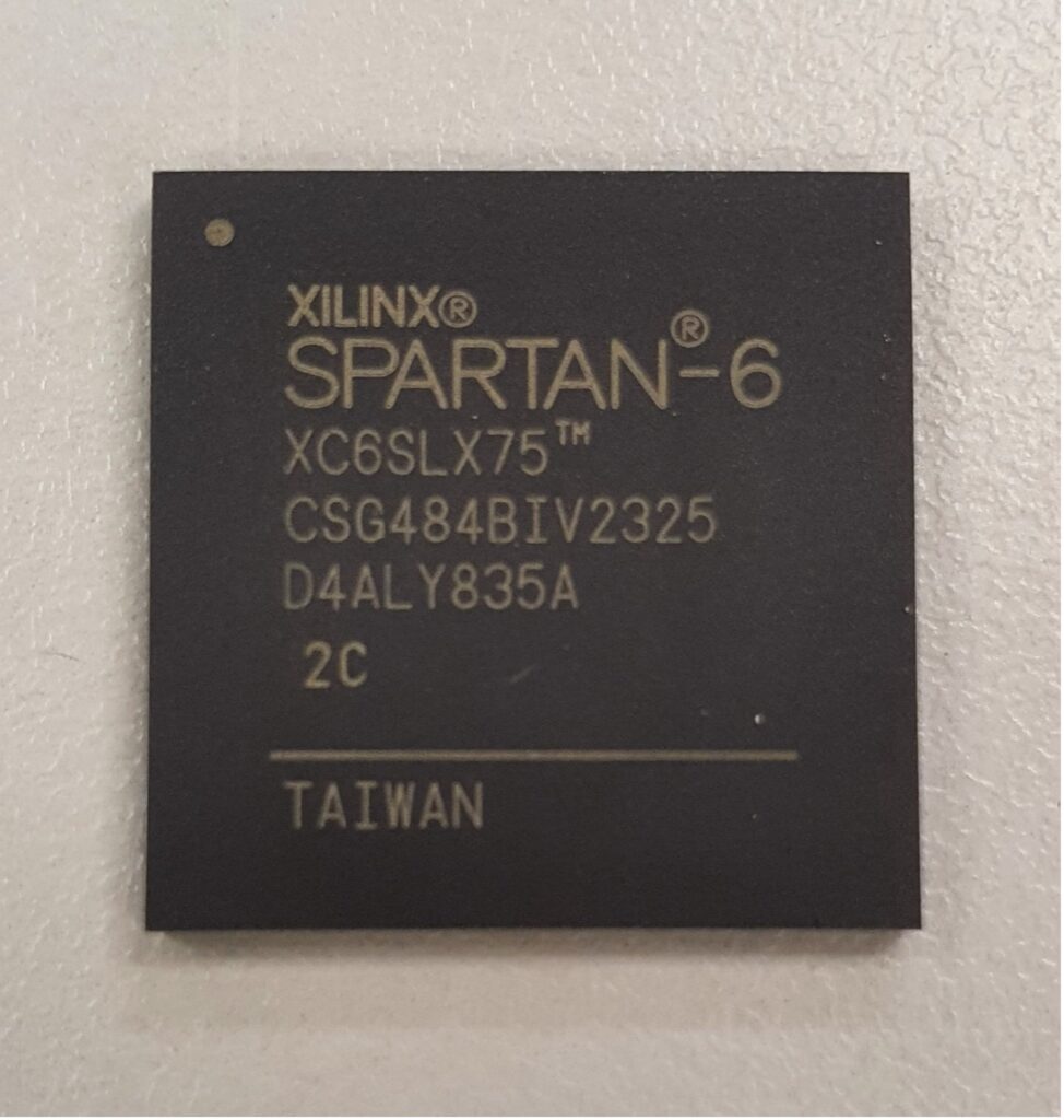
IOActive procured several Spartan 6 FPGAs from a respected supplier for a preliminary silicon teardown to gain insight into how the chip handles encrypted bitstreams and identify any other interesting features. As a standalone package, the Spartan chip looks like this:
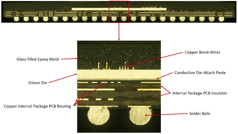
The CSG484 package that contains the Spartan 6 is a wire-bonded Ball-Grid Array (BGA) consisting of the IC die itself (face up), attached by copper ball bonds to a four-layer FR4 PCB substrate and overmolded in an epoxy-glass composite. The substrate has a grid of 22×22 solder balls at 0.8 mm pitch, as can be seen in the following cross section. The solder balls are an RoHS-compliant SAC305 alloy, unlike the “defense-grade” XQ6SLX75, which uses Sn-Pb solder balls. The choice of a consumer-grade FPGA for a military application is interesting, and may have been driven by cost or component availability issues (as the XQ series parts are produced in much lower volume and are not common in overseas supply chains).
The sample was then imaged in an SEM to gain insight into the metal layers for to order to perform refined deprocessing later. The chip logic exists on the surface of the silicon die, as outlined by the red square in the following figure.
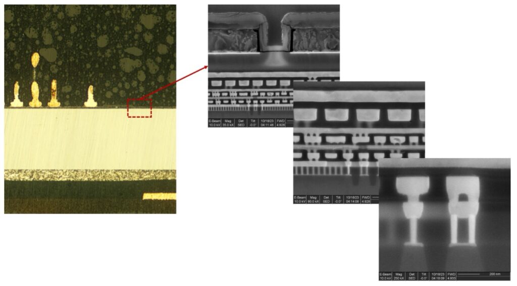
The XC6SLX75 is manufactured by Samsung on a 45 nm process with nine metal layers. A second FPGA was stripped of its packaging for a top-down analysis, starting with metal layer nine.
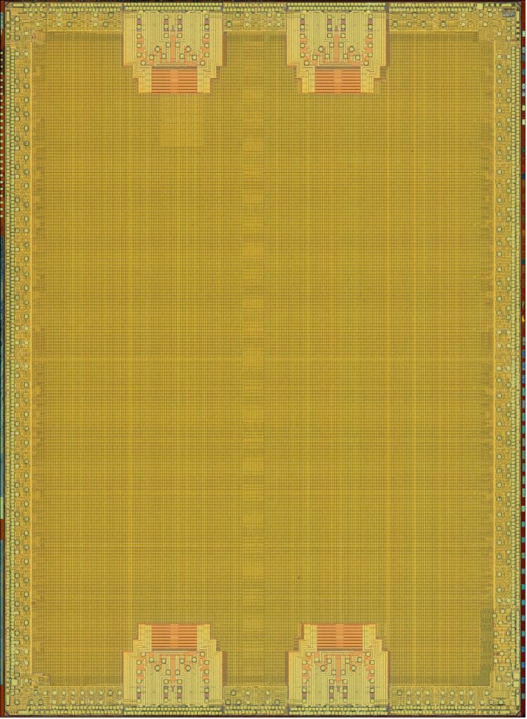
Looking at the top layer, not much structure is visible, as the entire device is covered by a dense grid of power/ground routing. Wire bond pads around the perimeter for power/ground and I/O pins can clearly be seen. Four identical regions, two at the top and two at the bottom, have a very different appearance from the rest of the device. These are pairs of multi-gigabit serial transceivers, GTPs in Xilinx terminology, capable of operation at up to 3.2 Gbps. The transceivers are only bonded out in the XC6SLX75T; the non –T version used in the radio does not connect them, so we can ignore them for the purposes of this analysis.
The metal layers were then etched off to expose the silicon substrate layer, which provides better insight into chip layout, as shown in the following figure.
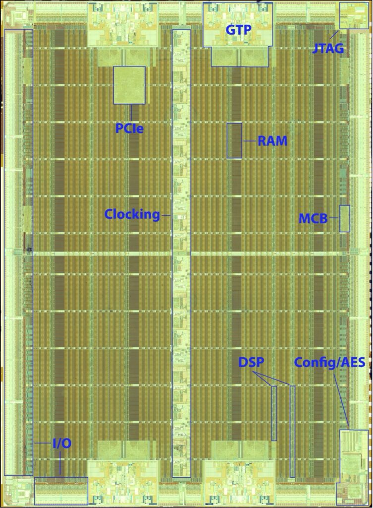
After etching off the metal and dielectric layers, a much clearer view of the device floorplan becomes visible. We can see that the northwest GTP tile has a block of logic just south of it. This is a PCIe gen1 controller, which is not used in the non –T version of the FPGA and can be ignored.
The remainder of the FPGA is roughly structured as columns of identical blocks running north-south, although some columns are shorter due to the presence of the GTPs and PCIe blocks. The non-square logic array of Spartan 6 led to poor performance as user circuitry had to be shoehorned awkwardly around the GTP area. Newer-generation Xilinx parts place the GTPs in a rectangular area along one side of the device, eliminating this issue.
The light-colored column at the center contains clock distribution buffers as well as Phase-Locked Loops (PLLs) and Digital Clock Managers (DCMs) for multiplying or dividing clocks to create different frequencies. Smaller, horizontal clock distribution areas can be seen as light-colored rows throughout the rest of the FPGA.
There are four columns of RAM containing a total of 172 tiles of 18 kb, and three columns of DSP blocks containing a total of 132 tiles, each consisting of an 18×18 integer multiplier and some other logic useful for digital signal processing. The remaining columns contain Configurable Logic Blocks (CLBs), which are general purpose logic resources.
The entire perimeter of the device contains I/O pins and related logic. Four light-colored regions of standard cell logic can be seen in the I/O area, two on each side. These are the integrated DDR/DDR2/DDR3 Memory Controller Blocks (MCBs).
The bottom right contains two larger regions of standard cell logic, which appear related to the boot and configuration process. We expect the eFuse and Battery-Backed SRAM (BBRAM), which likely contain the secrets required to decrypt the bitstream, to be found in this area. As such, this region was scanned in high resolution with the SEM for later analysis.

Utilizing advanced silicon deprocessing and netlist extraction techniques, IOActive hopes to refine methodologies for extracting the configured AES keys required to decrypt the bitstream that drives the Spartan 6 FPGA.
Once this is complete, there is a high probability that the unencrypted bitstream that configures the AZART can be obtained from a live radio and analyzed to potentially enumerate the secret encryption and frequency hopping algorithms that protect the current generation of AZART communications. We suspect that we could also apply this technique to previous generations of AZART, as well as other FPGA-based SDRs like those commonly in use by law enforcement, emergency services, and military operations around the world.


