INSIGHTS | September 13, 2008

Reverse-Engineering Custom Logic (Part 1)

Today we are taking you one step deeper into a microchip than we usually go. We look at transistors and the logic functions they compose, which helps us understand custom ASICs now found in some secured processors.

To reverse-engineer the secret functionality of an ASIC, we identify logic blocks, map out the wiring between the blocks, and reconstruct the circuit diagram. Today, we’ll only be looking at the first step: reading logic. And we start with the easiest example of a logic function: the inverter.

To read logic, you first have to find the transistors and decide where Vcc (+) and ground (-) are located. Transistors are easy to spot. They will always look very similar to those two transistors marked in the picture: A rectangle shape with a line in the middle. Vcc is always next to the larger transistors (PMOS) and ground is closer to the smaller ones (NMOS).

Once you identified the transistors, you draw a small circuit diagram that shows how they are connected to each other. In the example, the inputs of the two transistors are connected and so are their outputs on the left side. From this circuit diagram you can read that whatever you assert at the input, the output will be forced to the opposite state — an inverter.

Every gate will follow these basic principles, but vary in the number and constellation of transistors. A 2-NOR gate (Y = !(A|B) ), for instance, is composed of 4 transistors in this setup:

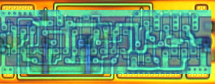
Once you figured out a gate, you can recognize every occurrence of that function on the whole chip because the exact same shape is always used for the same function. Generally, you only need to read a few dozens gates at most to generate a map of functions across whole chip. Get a head start on reading logic and check out the logic gate collection at The Silicon Zoo.

Here is a challenge for you to try (open in GIMP or Photoshop and toggle between the different layers):

It’s about the hardest function found on most chips with a total of 34 transistors, 3 inputs, 2 outputs, and time-variant behavior. The solution will be posted next week.

INSIGHTS |

New Author: Herr Karsten Nohl!

We are proud to announce that those who enjoy reading the blog (which we apologize for the lack of content lately) can soon enjoy reading posts from Karsten Nohl as well.

For those of you who are not familiar with Karsten, he played an important role in the discovery and analysis of the Crypto-1 mathematical algorithm found in Philips (NXP) Mifare RFID devices.

He recently obtained his PhD from University of Virginia in the United States.   He’s well known within the Chaos Computer Club (CCC) in Germany as well.

We too look forward to reading Karsten’s posts.   Feel free to give Karsten a round of applause by posting a quick comment!

Karsten- Congratulations on your PhD!!

INSIGHTS | April 3, 2008

Atmel AT91SAM7S Overview

Atmel produces a number of ARM based devices in their portfolio of products. We had one laying around the lab so here we go as usual…

The device was a 48 pin QFP type package. We also purchased a sample of the other members of the family although the initial analysis was done on the AT91SAM7S32 part shown above. All pictures will relate to this specific part even though there is not a signifigant difference between the other members of this line except memory sizes.

After decapsulating the die from inside the QFP, we find a beautifully layed out 210nm 5 metal design! Thats right, 5 metal layers! Strangely enough, we would have thought this was a 220nm 5 metal but apparently Atmel doesn’t have a .22um process so this is matching their .21um.

The core runs at 1.8v and allows 1.65v operation (thus it is their ATC20 process being used). The datasheet on the device can be found here. The 32KB Flash part also contains 8KB of SRAM (that’s a lot of ram!).

Notice on this particular layout, there is CMP filler metal (e.g. dead metal, metal slugs that are not connected to anything floating in SIO2) covering almost the entire die.

The picture above actually has had the top 2 metal layers removed. Metal 5 (M5) being the highest with the CMP filler and some power planes. Metal 4 (M4) had additional power planes and routing wires.

With Metals 1-3 still present, we can get a nice overview of the floorplan now. We can see the Flash, Fuses, and SRAM clearly. The Flash has a solid coating of metal over the entire cell area which has become common from Atmel to prevent UV light attacks we suppose?

We can now label the areas on the original top metal overview photo. There is a small boot-rom loader present on the device as well and is explained in the manual.

These cells were actually on Metal 1 and 2 but there are connections via Metal 3 as well.

There were additional power planes across the lower area of the photo from Metal 4 and 5 that cover those fuses however this isn’t buying them any security if the actual lock bits were buried there. A laser can go right through it all keeping the power-bus in tact with a hole in it.

In summary, this is a very well secured device. Fuses buried in a 5 metal layer design make the Microchip DSPIC’s look like a piece of cake in comparision (They are 350nm 4 metal).

We didn’t test this, but we are sure UV will set this fuses to a bad state if you can get the light to the floating gate since most all Atmel’s behave this way.

Nice job Atmel!

INSIGHTS | February 13, 2008

Atmel CryptoMemory AT88SC153/1608 :: Security Alert

A “backdoor” has been discovered by Flylogic Engineering in the Atmel AT88SC153 and AT88SC1608 CryptoMemory.

Before we get into this more, we want to let you know immediately that this backdoor only involves the AT88SC153/1608 and no other CryptoMemory devices.

The backdoor involves restoring an EEPROM fuse with Ultra-Violet light (UV).  Once the fuse bit has been returned to a ‘1’, all memory contents is permitted to be read or written in the clear (unencrypted).

Normally in order to do so, you need to either authenticate to the device or use a read-once-given “secure code” as explained in the AT88SC153 datasheet and the AT88SC1608 datasheet.

For those of you who are unfamiliar Atmel’s CryptoMemory, they are serial non-volatile memory (EEPROM) that support a clear or secure channel of communications between a host (typically an MCU) and the memory.  What is unique about the CryptoMemory are their capabilities in establishing the secure channel (authenticating to the host, etc).

These device includes:

High-security Memory Including Anti-wiretapping

64-bit Authentication Protocol

Secure Checksum

Configurable Authentication Attempts Counter

These device includes:

  • Multiple Sets of Passwords
  • Specific Passwords for Read and Write
  • Password Attempts Counters
  • Selectable Access Rights by Zone
  • High-security Memory Including Anti-wiretapping
  • 64-bit Authentication Protocol
  • Secure Checksum
  • Configurable Authentication Attempts Counter

Section 5 of the datasheet labled, “Fuses” clearly states, “Once blown, these EEPROM fuses can not be reset.

This statement is absolutely false.  UV light will erase the fuses back to a ‘1’ state.  Care must be used to not expose the main memory to the UV or else it too will erase itself.

We are not going to explain the details of how to use the UV light to reset the fuse.  We have tried to contact Atmel but have not heard anything back from them.

Reading deeper into the datasheet under Table 5-1, Atmel writes, “When the fuses are all “1”s, read and write are allowed in the entire memory.

As strange as it reads, they really do mean even if you have setup security rules in the configuration memory, it doesn’t matter.  The fuses override everything and all memory areas are readable in the clear without the need for authentication or encrypted channel!  The attacker can even see what the “Secure Code” is (it is not given out in the public documentation, nor with samples).  Atmel was even kind enough to leave test pads everywhere so various levels of attackers can learn (entry to expert).

Our proof of concept was tested on samples we acquired through Atmel’s website.  Atmel offers samples to anyone however they do not give out the “Secure code” as mentioned above.
  • The secure code of the AT88SC153 samples was “$D_ $F_ $7_”.
  • The secure code of the AT88SC1608 was “$7_ $5_ $5_”.

We are not going to show you the low nibble of the 3 bytes to make sure we don’t give the code out to anyone.  This is enough proof to whoever else knows this code.  That person(s) can clearly see we know their transport code which appears to be common to all samples (e.g. All die on a wafer contain the same secure code until a customer orders parts at which time that customer receives their own secure code.).  A person reading this cannot guess the secure code in because there are 12 bits to exhaustively search out and you only have 8 tries ;).

Of all the other CryptoMemory products, only the AT88SC153/1608 has this backdoor.  We have successfully analyzed the entire CryptoMemory product line and can say that the backdoor doesn’t exist in any other CryptoMemory part.  None of the CryptoMemory parts are actually as “secure” as they make it seem.  The words, “Smoke n’ Mirrors” comes to mind (It is almost always like that).  In this particular category of CryptoMemory, there are two parts, the AT88SC153 and the larger AT88SC1608.

Thus the questions-
    • Why has Atmel only backdoored this part (NSA for you conspiracists)?
    • Who was the original intended customer supposed to be?
    • Was the original intention of these devices to be used in a product that used some kind of cryptography?

If the above was true, was this device originally intended to be a cryptographic key-vault?

All these questions come to mind because the backdoor makes it so easy to extract the contents of the device they want you to trust.  Some of you may be familiar with the GSM A5/1 algorithm having certain bits of the key set to a fixed value.

Judging by the wording of the documentation, Atmel gives the appearance that CryptoMemory are the perfect choice for holding your most valuable secrets.

Give us your thoughts…

INSIGHTS | February 7, 2008

AT90S8515 – Legacy!

Some people asked for some of those older Atmel parts after seeing the MEGA88 and ATMEGA169 teardowns.

Here’s a quick one on the AT90S8515. It’s still very popular even though it’s been replaced by the MEGA8515. It’s built on a larger process and it’s not planarized (.50um and below are planarized but you may find some .50um non-planarized)

8KB Flash, 512 Byte SRAM, 512 Byte EEPROM with 32 working registers. That’s sooo nice! 4x faster than the typical PIC.

There was a mistake in the above picture too when we highlighted the areas! We forgot to outline the EEPROM area.

The side of the array is touching the ‘8’ in 8KB EEPROM above and it runs vertical along-side the FLASH. So in theory there are two 8 bit FLAH arrays and a single 8 bit EEPROM area all running veritical in the “8KB Flash” highlighted area.

Give us your feedback!

INSIGHTS | January 24, 2008

ATMEGA88 Teardown

An 8k FLASH, 512 bytes EEPROM, 512 bytes SRAM CPU operating 1:1 with the external world unlike those Microchip PIC’s we love to write up about :).

It’s a 350 nanometer (nm), 3 metal layer device fabricated in a CMOS process.  It’s beautiful to say the least;  We’ve torn it down and thought we’d blog about it!

The process Atmel uses on their .35 micrometer (um) technology is awesome.

Using a little HydroFluoric Acid (HF) and we partially removed the top metal layer (M3).  Everything is now clearly visible for our analysis. After delaying earlier above, we can now recognize features that were otherwise hidden such as the Static RAM (SRAM) and the 32 working registers.

As we mentioned earlier, we used the word, “awesome” because check this out- It’s so beautifully layed out that we can etch off just enough of the top metal layer to leave it’s residue so it’s still visible depending on the focal point of the microscope!  This is very important.

We removed obscuring metal but can still see where it went (woot!).The two photos above contain two of the 30+ configuration fuses present however it makes a person wonder why did Atmel cover the floating gate of the upper fuse with a plate of metal (remember the microchip article with the plates over the floating gates?)

We highlighted a track per fuse in the above photos.  What do you think these red tracks might represent?

INSIGHTS | January 22, 2008

Security Mechanism of PIC16C558,620,621,622

Last month we talked about the structure of an AND-gate layed out in Silicon CMOS.  Now, we present to you how this AND gate has been used in Microchip PICs such as PIC16C558, PIC16C620, PIC16C621, PIC16C622, and a variety of others.

If you wish to determine if this article relates to a particular PIC you may be in possession of, you can take an windowed OTP part (/JW) and set the lock-bits.  If after 10 minutes in UV, it still says it’s locked, this article applies to your PIC.

IF THE PART REMAINS LOCKED, IT CANNOT BE UNLOCKED SO TEST AT YOUR OWN RISK.

The picture above is the die of the PIC16C558 magnified 100x.  The PIC16C620-622 look pretty much the same.  If there are letters after the final number, the die will be most likely, “shrunk” (e.g. PIC16C622 vs PIC16C622A).

Our area of concern is highlighted above along with a zoom of the area.

When magnified 500x, things become clear.  Notice the top metal (M2) is covering our DUAL 2-Input AND gate in the red box above.We previously showed you one half of the above area.  Now you can see that there is a pair of 2-input AND gates.  This was done to offer two security lock-bits for memory regions (read the datasheet on special features of the CPU).Stripping off that top metal (M2) now clearly shows us the bussing from two different areas to keep the part secure.  Microchip went the extra step of covering the floating gate of the main easilly discoverable fuses with metal to prevent UV from erasing a locked state.  The outputs of those two fuses also feed into logic on the left side of the picture to tell you that the part is locked during a device readback of the configuration fuses.

This type of fuse is protected by multiple set fuses of which only some are UV-erasable.

The AND gates are ensuring all fuses are erased to a ‘1’ to “unlock” the device.

What does this mean to an attacker?  It means, go after the inal AND gate if you want to forcefully unlock the CPU.  The outputs of the final AND gate stage run underneather VDD!! (The big mistake Microchip made).  Two shots witha laser-cutter and we can short the output stages “Y” from the AND-gate to a logic ‘1’ allowing readback of the memories (the part will still say it is locked).Stripping off the lower metal layer (M1) reveils the Poly-silicon layer.

What have we learned from all this?

    • A lot of time and effort went into the design of this series of security mechanisms.
    • These are the most secure Microchip PICs of ALL currently available.  The latest ~350-400nm 3-4 metal layer PICs are less secure than the
    • Anything made by human can be torn down by human!

:->

INSIGHTS | December 29, 2007

AND Gates in logic

As we prepare for the New Year, we wanted to leave you with a piece of logic taken out of an older PIC16C series microcontroller. We want you to guess which micro(s) this gate (well the pair of them) would be found in. After the New Year, we’ll right up on the actual micro(s) and give the answer :).

An AND gate in logic is basically a high (logic ‘1’) on all inputs to the gate. For our example, we’re discussing the 2 input AND. It should be noted that this is being built from a NAND and that a NAND would require 2 less gates than an AND.

The truth table is all inputs must be a ‘1’ to get a ‘1’ on the output (Y). If any input is a ‘0’, Y = ‘0’.

There are 2 signals we labeled ‘A’ and ‘B’ routed in the Poly layer of the substrate (under all the metal). This particular circuit is not on the top of the device and had another metal layer above it (Metal 2 or M2). So technically, you are seeing Metal 1 (M1) and lower (Poly, Diffusion).

It’s quickly obvious that this is an AND gate but it could also be a NAND by removing the INVERTER and taking the ‘!Y’ signal instead of ‘Y’.

The red box to the left is the NAND leaving the red box to the right being the inverter creating our AND gate.

The upper green area are PFET’s with the lower green area being NFET’s.

After stripping off M1, we now can clearly see the Poly layer and begin to recognize the circuit.

This is a short article and we will follow up after the New Year begins. This is a single AND gate but was part of a pair. From the pair, this was the right side. We call them a pair because they work together to provide the security feature on some of the PIC16C’s we’re asking you to guess which ones 🙂

Happy Holidays and Happy Guessing!

INSIGHTS | December 17, 2007

ST201: ST16601 Smartcard Teardown

ST SmartCards 201 – Introduction to the ST16601 Secure MCU

This piece is going to be split into two articles-

    • The first being this article is actually a primer on all of the ST16XYZ series smartcards using this type of Mesh technology.  They have overgone a few generations.  We consider this device to be a 3rd generation.
    • In a seperate article yet to come, we are going to apply what you have read here to a smartcard used by Sun Microsystems, Inc. called Payflex.  From what we have gathered on the internet, they are used to control access to Sun Ray Ultra Thin Terminals.  Speaking of the payflex cards, they are commonly found (new and used) on eBay.

The ST16601 originated as far back as 1994.  It originally appeared as a 1.2 um, 1 metal CMOS process and was later shrunk to 0.90 um, 1 metal CMOS to support 2.7v – 5.5v ranges.

It appears to be a later generation of the earlier ST16301 processor featuring larger memories (ROM, RAM, EEPROM).

The ST16601 offers:

    • 6805 cpu core with a few additional instructions
    • Lower instruction cycle counts vs. Motorola 6805.
    • Internal Clock can run upto 5 Mhz at 1:1 vs 2:1.
    • 6K Bytes of ROM
    • 1K Bytes of EEPROM
    • 128 Bytes of RAM
    • Very high security features including EEPROM flash erase (bulk-erase)

Although it was released in 1994 it was being advertised in articles back in 1996.  Is it possible an ‘A’ version of the ST16601 was released without a mesh?  We know the ST16301 was so anything is possible.

Final revision of the ST16601(C?).  The part has been shrunk to 0.90um and now has ST’s 2nd generation mesh in place.  The newer mesh still in use today consists of fingers connected to ground and a serpentine sense line connected to power (VDD).

Using our delayering techniques, we removed the top metal mesh from the 1997 version of the part.  The part numbering system was changed in 1995 onward to not tell you what part something really is.  You have to be knowledgable about the features present and then play match-up from their website to determine the real part number.

As you can see, this part is clearly an ST16601 part except it is now called a K3COA.  We know that the ‘3’ represents the entire ST16XYZ series from 1995-1997 but we’ll get into their numbering system when we write the ST101 article (we skipped it and jumped straight to ST201 to bring you the good stuff sooner!).

Above:  1000x magnification of the beginning of the second generation mesh used ont he 1995+ parts.  This exact mesh is still used today on their latest technology sporting 0.18um and smaller!  The difference- the wire size and spacing.

In the above image, green is ground, red is connected to power (VDD).  Breaking this could result in loss of ground to a lower layer as well as the sense itself.  The device will not run with a broken mesh.

Flylogic has successfully broken their mesh and we did it without the use of a Focus Ion-Beam workstation (FIB).  In fact, we are the ONLY ONES who can open the ST mesh at our leisure and invasively probe whatever we want.  We’ve been sucessful down-to 0.18um.

Using our techniques we call, “magic” (okay, it’s not magic but we’re not telling 😉 ), we opened the bus and probed it keeping the chip alive.  We didn’t use any kind of expensive SEM or FIB.  The equipment used was available back in the 90’s to the average hacker!  We didn’t even need a university lab.  Everything we used was commonly available for under $100.00 USD.

This is pretty scary when you think that they are certifying these devices under all kinds of certifications around the world.

Stay tuned for more articles on ST smartcards.  We wanted to show you some old-school devices before showing you current much smaller ones because you have to learn to crawl before you walk!

INSIGHTS | December 1, 2007

Infineon SLE4442

The SLE4442 has been around for a long time.  Spanning a little more than 10 years in the field, it has only now began to be replaced by the  newer SLE5542 (We have analyzed this device too and will write up an article soon).

It is basically a 256 byte 8 bit wide EEPROM with special write protection.  In order to successfully write to the device, you need to know a 3 byte password called the Programmable Security Code (PSC).  The code is locked tightly inside the memory area of the device and if you try to guess it, you have 3 tries before being permanently locked out forever (well forever for some, we can always perform magic on the part).o above is a picture shows the entire substrate. 

There was still some dirt on the die but it didn’t effect our interests.  The geometry of the device is pretty big (> 2 uM).  It has one polysilicon layer and one metal layer fabricated using an NMOS process.

Note:  Just because the device is big does not constitute ease of an attack but it does make execution of an attack easier for an attacker without large amount of expense.

A successful attack on this device means an attacker knows the PSC which enables write operations to the device under attack or the ability to clone the device under attack into fresh new target who can act like the original device.  We’ll discuss the PSC in more detail below.We have pr identified all the important areas listed on the Page 7 diagram in the above picture.

We can see again a test circuit that has had its enable sawn off during production.  We can see the enable line looping back for the die that was placed to the right of this die.  Notice the duck?  Hrmmmm… Seems to be pointing at 2 test points.  We’ll just say that the duck probably knows what he’s looking at 😉

We removed the top metal (the only metal layer) and you can now see the diffusion and poly layers.  You can literally take these two pictures above and create a schematic from them if you understand NMOS circuits.

Possible attacks on the device:

    • Electrical glitches:  Fed through VCC / CLOCK line are possible.  The circuit latches are all toggled from the serial clock provided by the user.
    • Optical Erasure:  UV seems to clear cells of the EEPROM to zero.  Masking of the EEPROM except for the 3 PSC bytes would result in a PSC of $00,$00,$00 for that particular device.  However note this is not a favorable attack as the device would probably become rejected by the host that this device belongs too.
    • Optical glitches:  These give strange results.  An optical glitch in the right area might produce readback of the PSC code through command $31 (Read Security Memory).
    • Bus attacks:  Sitting on the databus will show you the PSC of the device.  This method is effective but not easilly accomplish by most.
    • PSC Control logic:  Find the right signal in this area and you can make the device believe a valid PSC has been previously given allowing readback of the PSC through command $31.  This is our prefered method, just ask the duck ;).

The security model used on this type of device is one in which the host-environment is trusted.  This is a risky way of thinking but ironically, it has been used a lot (Fedex/Kinko’s payment cards(SLE4442, SLE5542), Telephone cards in use worldwide (ST1335, ST1355), laundry machine smartcards (AT88SC102).

Proof of failure of this trust model has been shown in places such as:

    • Phone card emulation in Europe.  It became so bad, metal detectors were placed inside the phones smartcard area to deter eavesdropping.
    • Fedex/Kinko’s was successfully compromised by a man named Strom Carlson.  He demonstrated the abuse of the SLE4442 in use by Kinko’s at the time.