INSIGHTS | February 3, 2012

Solving a Little Mystery

Firmware analysis is a fascinating area within the vast world of reverse engineering, although not very extended. Sometimes you end up in an impasse until noticing a minor (or major) detail you initially overlooked. That’s why sharing methods and findings is a great way to advance into this field.

While looking for certain information during a session of reversing, I came across this great post. There is little to add except for solving the ‘mystery’ behind that simple filesystem and mentioning a couple of technical details.
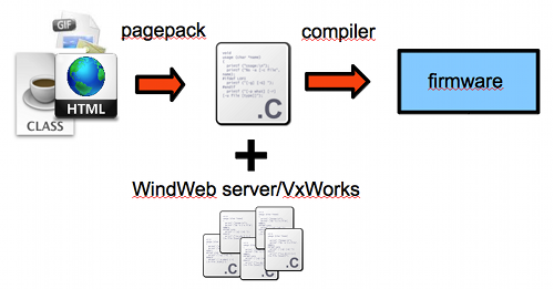
This file system is part of the WindRiver’s Web Server architecture for embedded devices, so you will likely find it inside firmwares based on VxWorks. It is known as MemFS (watch out, not the common MemFS) or Wind River management file system, and basically allows devices to serve files via the embedded web server without needing an ‘actual’ file system since this one lies on its non-volatile memory.
VxWorks  provides  pagepack, a tool used to transform any file intended to be served by a WindWeb server into C code. Therefore, a developer just compiles everything into the same firmware image.
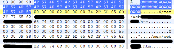
 From a reverser’s point of view, what we should find is the following structure:


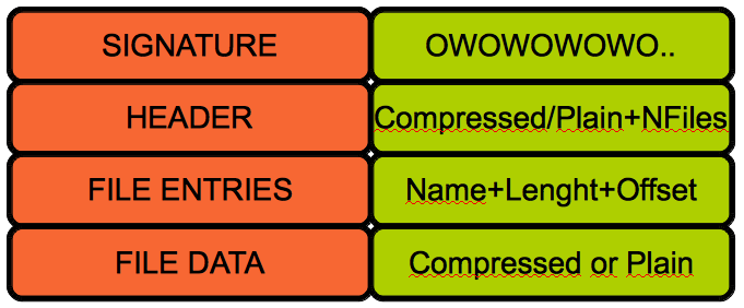
 There are a few things  here worth mentioning:

  • The header is not necessarily 12 but 8 so the third field seems optional.
  • The first 4 bytes look like a flag field that may indicate, among other things,  whether  a file data will be compressed or not (1 = Compressed, 2 = Plain)
  • The signature can vary between firmwares since it is defined by the constant ‘HTTP_UNIQUE_SIGNATURE’ , in fact, we may find this signature twice inside a firmware; the first one due to  the .h  where it is defined (close to other strings such as the webserver banner )and the second one already as part of  the MemFS.
Hope these additional details help you on your future research.
INSIGHTS | August 7, 2010

Parallax Propeller P8X32A Quick Teardown

Parallax has a really neat 8 core 32 bit CPU called the ‘Propeller’.  It’s been out for a few years but it is gaining popularity.  There is no security with the device as it boots insecurely via a UART or I2C EEPROM.  None the less, we thought it was interesting to see an 8 core CPU decapsulated!

One can clearly see 8 columns that appear almost symmetric (except in the middle region).  The upper 8 squares are each ‘cogs’ 512 * 32 SRAMs as described in the manual.  The middle left 4 and right 4 squares are the ROM’s Parallax describes.  The 8 rectangular objects are the 32KB SRAM as described.  The 8 cores are basically the 8 columns above the middle ROM’s to include the 512 * 32 SRAMs because they describe each cog as having it’s own 512 * 32 SRAM :).

Last but not least is the logo by Parallax.  Nice job Parallax on this beast!  We have one favor-  implement some flash on the next generation with a security bit ;).

INSIGHTS | January 24, 2008

ATMEGA88 Teardown

An 8k FLASH, 512 bytes EEPROM, 512 bytes SRAM CPU operating 1:1 with the external world unlike those Microchip PIC’s we love to write up about :).

It’s a 350 nanometer (nm), 3 metal layer device fabricated in a CMOS process.  It’s beautiful to say the least;  We’ve torn it down and thought we’d blog about it!

The process Atmel uses on their .35 micrometer (um) technology is awesome.

Using a little HydroFluoric Acid (HF) and we partially removed the top metal layer (M3).  Everything is now clearly visible for our analysis. After delaying earlier above, we can now recognize features that were otherwise hidden such as the Static RAM (SRAM) and the 32 working registers.

As we mentioned earlier, we used the word, “awesome” because check this out- It’s so beautifully layed out that we can etch off just enough of the top metal layer to leave it’s residue so it’s still visible depending on the focal point of the microscope!  This is very important.

We removed obscuring metal but can still see where it went (woot!).The two photos above contain two of the 30+ configuration fuses present however it makes a person wonder why did Atmel cover the floating gate of the upper fuse with a plate of metal (remember the microchip article with the plates over the floating gates?)

We highlighted a track per fuse in the above photos.  What do you think these red tracks might represent?

INSIGHTS | January 22, 2008

Security Mechanism of PIC16C558,620,621,622

Last month we talked about the structure of an AND-gate layed out in Silicon CMOS.  Now, we present to you how this AND gate has been used in Microchip PICs such as PIC16C558, PIC16C620, PIC16C621, PIC16C622, and a variety of others.

If you wish to determine if this article relates to a particular PIC you may be in possession of, you can take an windowed OTP part (/JW) and set the lock-bits.  If after 10 minutes in UV, it still says it’s locked, this article applies to your PIC.

IF THE PART REMAINS LOCKED, IT CANNOT BE UNLOCKED SO TEST AT YOUR OWN RISK.

The picture above is the die of the PIC16C558 magnified 100x.  The PIC16C620-622 look pretty much the same.  If there are letters after the final number, the die will be most likely, “shrunk” (e.g. PIC16C622 vs PIC16C622A).

Our area of concern is highlighted above along with a zoom of the area.

When magnified 500x, things become clear.  Notice the top metal (M2) is covering our DUAL 2-Input AND gate in the red box above.We previously showed you one half of the above area.  Now you can see that there is a pair of 2-input AND gates.  This was done to offer two security lock-bits for memory regions (read the datasheet on special features of the CPU).Stripping off that top metal (M2) now clearly shows us the bussing from two different areas to keep the part secure.  Microchip went the extra step of covering the floating gate of the main easilly discoverable fuses with metal to prevent UV from erasing a locked state.  The outputs of those two fuses also feed into logic on the left side of the picture to tell you that the part is locked during a device readback of the configuration fuses.

This type of fuse is protected by multiple set fuses of which only some are UV-erasable.

The AND gates are ensuring all fuses are erased to a ‘1’ to “unlock” the device.

What does this mean to an attacker?  It means, go after the inal AND gate if you want to forcefully unlock the CPU.  The outputs of the final AND gate stage run underneather VDD!! (The big mistake Microchip made).  Two shots witha laser-cutter and we can short the output stages “Y” from the AND-gate to a logic ‘1’ allowing readback of the memories (the part will still say it is locked).Stripping off the lower metal layer (M1) reveils the Poly-silicon layer.

What have we learned from all this?

    • A lot of time and effort went into the design of this series of security mechanisms.
    • These are the most secure Microchip PICs of ALL currently available.  The latest ~350-400nm 3-4 metal layer PICs are less secure than the
    • Anything made by human can be torn down by human!

:->

INSIGHTS | November 15, 2007

The KEYLOK USB Dongle. Little. Green. And dead before it was born!

We decided to do a teardown on a Keylok USB based dongle from Microcomputer Applications, Inc. (MAI).

Opening the dongle was no challenge at all. We used an x-acto knife to slit the sidewall of the rubber protective coating. This allowed us to remove the dongle’s circuit board from the surrounding protective coating.

The top side of the printed circuit board (PCB) is shown above. MAI did not try to conceal anything internally. We were a little surprised by this :(.

The backside consists of two tracks and a large ground plane. The circuit is very simple for an attacker to duplicate.

With the devices removed, a schematic can be created literally within minutes. The 20-pin version of CY7C63101A can even be used in place of the smaller SOIC 24-pin package (which is difficult for some to work with). The 20-pin is also available in a dual-inline-package (DIP) making it a great candidate for an attacker to use.

Red pin denotes pin 1 on the device.

We performed some magic and once again we have success to unlock the once protected device. A quick look for ASCII text reveals a bunch of text beginning around address $06CB: .B.P.T. .E.n.t.e.r.p.r.i.s.e.s…D.o.n.g.l.e. .D.o.n.g.l.e. .C.o.m.m.<
.E.n.d.P.o.i.n.t.1. .1.0.m.s. .I.n.t.e.r.r.u.p.t. .P.i.p.e.

Ironically, they say, “There are many advantages to using a hardware “based security solution AKA, a Dongle. There are even more advantages however to using KEYLOK Dongles over other competing solutions.”

Statement’s such as the one above are the reason Flylogic Engineering started this blog. We have heard this just one too many times from companies who are franckly pushing garbage. Garbage in, garbage out. Enough said on that.

This dongle is the weakest hardware based security token we have ever seen!! The outer physical protection layers ease of entry places this dongle last on our list of who’s hot and who’s not!

INSIGHTS | October 26, 2007

Decapsulated devices

Recently at Toorcon9 (www.toorcon.org), some individuals asked to see images of decapsulated parts still in their packages. I dug around and came up with some examples. Click on any of the pictures for a larger version.

Above: Dallas DS89C450
Above: Microchip dsPIC30F6013

Using our proprietary procedures, all parts remain 100% functional with no degradation after exposing the substrate.