
Key Takeaways
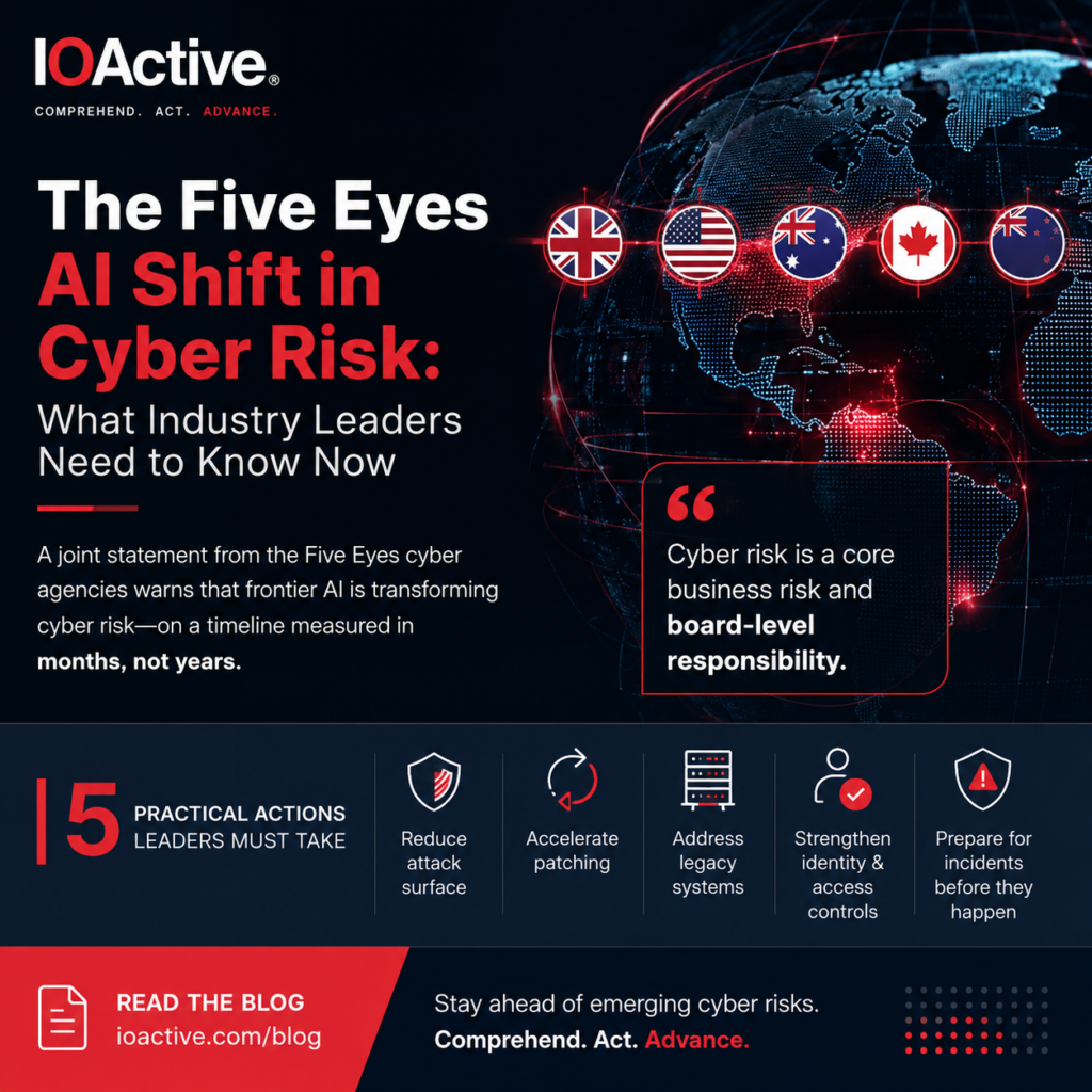
- On 22 June 2026, the leaders of the Five Eyes cyber security agencies issued a joint statement, The AI Shift in Cyber Risk: Why Leaders Must Act Now, warning that frontier AI is transforming cyber risk on a timeline measured in months, not years.
- The statement is signed by the heads of the National Cyber Security Centre (NCSC, UK), Cybersecurity and Infrastructure Security Agency (CISA, US), National Security Agency (NSA, US), Australian Signals Directorate (ASD, Australia), Communications Security Establishment (CSE, Canada), and Government Communications Security Bureau (GCSB, New Zealand) — an unusually unified articulation of urgency from the Five Eyes partnership.
- Cyber risk is explicitly reframed as a core business risk and board-level responsibility, not a technical issue to be delegated downward.
- Five practical actions are prescribed: reduce attack surface, accelerate patching, address legacy systems, strengthen identity and access controls, and prepare for incidents before they happen.
- The statement lands days after the NCSC’s own CEO disclosed that 75% of attacks on UK critical infrastructure over the past year are linked to hostile states, and weeks after NCSC guidance warning of an incoming “vulnerability patch wave” driven by AI-accelerated exploitation.
- Organisations that treat this as a compliance afterthought will be out of step with where their regulators, and their adversaries, are already heading.
A Statement for a Narrowing Window
Joint statements from the Five Eyes cyber agencies are not issued lightly, and this one is notable for its tone as much as its content. Published on 22 June 2026, The AI Shift in Cyber Risk [1] is signed jointly by Stephanie Crowe (ASD), Rajiv Gupta (CSE), Catriona Robinson (GCSB), Richard Horne (NCSC), David Imbordino (NSA), and Nick Andersen (CISA). The framing is unambiguous: frontier AI models are expected to exceed current industry expectations, and the timeline for that shift is not years, it is months.
This is not an isolated warning. Five days before the statement was published, NCSC CEO Dr Richard Horne told the Royal United Services Institute’s Annual Security Lecture that the NCSC had managed more than 200 cyber incidents affecting the UK’s critical national infrastructure in the year to May 2026, with around 75% believed linked to hostile state actors including Russia, China, and Iran [2]. Horne went further, arguing that cyber security should no longer be framed as a risk to be tolerated within appetite, but as an ongoing contest with capable adversaries. He also pointed to an NCSC assessment that by 2028, AI-enabled capabilities will likely be used to exploit known vulnerabilities in legacy technology at scale across UK critical infrastructure.
That assessment builds directly on guidance the NCSC published in May 2026, warning organisations to prepare for a “vulnerability patch wave”: a forced correction in which AI-accelerated exploitation surfaces decades of accumulated technical debt across commercial, open source, and proprietary software simultaneously [3]. The Five Eyes statement should be read as the international consolidation of that warning, not a standalone development.
What Does the Statement Set Out?
The statement is short and deliberately free of new technical detail. Its purpose is to compress urgency into a small number of leadership-level actions, structured around four overarching asks and five practical steps [1].
Leaders are urged to:
- Understand and assess risk, readiness, and accountability. Boards need a clear, current picture of organisational exposure, not a static risk register reviewed annually.
- Prioritise foundational cyber security practices and controls. Sophistication in tooling does not substitute for getting the fundamentals right.
- Empower cyber leaders with authority and resources. Cyber leadership requires the mandate to act, not just the responsibility to report.
- Stay actively engaged as threats and guidance evolve. Static governance models cannot keep pace with a threat landscape that is itself accelerating.
Two structural points distinguish this statement from prior Five Eyes guidance. First, it reframes AI not solely as an adversary capability but as a defensive obligation: organisations are explicitly told to use AI deliberately to strengthen defence, not merely to improve efficiency. Second, it sets an expectation that breaches are not preventable in absolute terms; preparedness is reframed as the capability to contain incidents quickly before they escalate into operational and financial crises [1].
Who is Affected by the Statement?
Boards and Executive Leadership
The statement is addressed primarily upward, not downward. It states plainly that cyber resilience is not an IT issue, it is central to operational continuity and market trust, and that it is not enough to have controls; leaders must be confident those controls will perform during a real incident [1]. This places direct accountability on boards and executives to verify resilience, not simply to fund it.
CISOs and Security Leadership
For security leaders, the statement is a mandate to escalate. The call to empower cyber leaders with authority and resources [1] gives CISOs a clear external reference point when seeking budget, headcount, or the organisational authority to challenge unsafe trade-offs that have previously been accepted in the name of operational convenience.
Operators of Critical National Infrastructure
For CNI operators, the statement reinforces direction already set domestically. The NCSC’s own intervention five days prior, disclosing that three-quarters of attacks on UK CNI are state-linked [2], makes clear that the threat described in the Five Eyes statement is not a future scenario for this sector. It is the current operating environment.
Vendors and Technology Providers
The statement explicitly calls on leaders across industry, including vendors, to act now [1]. Combined with the NCSC’s separate warning that a wave of vulnerability disclosures is approaching across commercial, open source, and proprietary software [3], vendors should expect both faster exploitation of existing flaws and intensifying customer expectations around patch velocity and secure-by-design practice.
What are the Key Challenges Organisations Will Face?
Compressed Exploitation Timelines
The central technical claim underpinning the statement is that AI is shrinking the window between vulnerability discovery and exploitation [1]. Patch cadences and change-management processes built around weeks or months of lead time were not designed for this. Organisations with manual patching processes, particularly across operational technology environments with long update cycles, face a widening gap between the speed of the threat and the speed of their own response.
Your Adversary Already Has an AI Upgrade
Even if your organization hasn’t touched AI, your attackers have. The patch window that once gave defenders breathing room is effectively gone — Mandiant’s time-to-exploit tracking shows exploits now landing on or before the day a CVE goes public. Exploitation itself has become a commodity: working proof-of-concept exploits can be generated in about 15 minutes, and autonomous vulnerability discovery campaigns can be run for roughly $50. This isn’t theoretical. Recovered logs from a June incident (via OALABS) showed a single operator driving over 1,000 AI-agent sessions across 14+ companies, with the models flagging a policy violation only about 10 times — because every request was simply framed as “authorized red-team” work. Social engineering has scaled right alongside it: Arup lost $25.6 million in 2024 after a video call where every “colleague” on the line was a deepfake, and the economics of that kind of attack have only gotten cheaper since. None of this requires exotic new attack vectors. It’s the same attack surface organizations have always had, now facing an adversary that doesn’t sleep, doesn’t hesitate, and operates at machine speed.
Legacy and Unsupported Systems
The statement is blunt that unsupported systems are not just technical debt, they are strategic liabilities [1]. This sits uncomfortably with sectors where legacy estate is structural rather than incidental, where replacement cycles are measured in years and safety-critical considerations constrain how quickly systems can be patched or retired.
Governance Gaps Between Boards and Technical Teams
Repeated emphasis on board-level accountability assumes a level of cyber literacy that many boards do not yet have. The gap between technical risk and the language boards use to govern it remains one of the most persistent obstacles to the kind of confident assurance the statement demands.
AI as a Dual-Use Capability
The statement’s insistence that organisations use AI deliberately to strengthen defence, not just improve efficiency [1], is a meaningfully higher bar than most organisations’ current AI security posture. Many security teams have adopted AI tooling for productivity gains. Far fewer have built the detection, monitoring, and response capability the statement envisages, while simultaneously managing the new attack surface that frontier AI systems themselves introduce.
Shipping Faster Means Shipping More Attack Surface
AI coding assistants have undeniably accelerated software delivery — but speed and security are moving in opposite directions. Veracode’s testing across more than 100 models found that roughly 45% of AI-generated code carries a security weakness. What’s more concerning is the trendline: functional correctness has raced past 95%, while the security rate has stayed flat at around 55% for two years running. Newer, smarter models are writing code that works — not code that’s safe. The practical impact is that attack surface is now growing at delivery speed, with code merging faster than any human review process was designed to handle, whether that code was sanctioned by the organization or introduced through shadow AI use, often with no clear provenance to trace it back. At the same time, client appetite for security testing is rising faster than budgets are — creating a widening gap between how much validation organizations want and how much they’re actually resourcing. Closing that appetite-budget gap is, in many ways, the central challenge facing security teams right now.
Zero-Day Proliferation
The statement warns directly that as AI systems evolve, new and previously unknown vulnerabilities will emerge, including zero-day vulnerabilities [1]. Defence-in-depth, rather than reliance on any single control or technology, is positioned as the only credible response to a vulnerability landscape that is itself becoming less predictable.
How IOActive Can Help
IOActive’s work across offensive security, operational technology and industrial control system (OT/ICS) assessment, and critical infrastructure advisory positions us to support organisations translating this statement’s leadership-level mandate into operationally credible defence. Testing, not assumption, is how organisations find out whether their controls will actually perform under pressure, which is precisely the bar the statement sets.
Red Team and Purple Team Services
The statement’s call to verify that controls will perform during a real incident, not merely exist on paper [1], is best answered through adversarial testing rather than compliance review. IOActive’s Red Team operations emulate the tactics of the threat actors most likely to target a given organisation’s sector and assets, while our Purple Team engagements translate offensive findings directly into measurable improvements in detection and response.
Full Stack Security Assessments
Reducing attack surface and accelerating patching, two of the statement’s five practical actions [1], both depend on first knowing where exposure actually sits. Our full stack assessments examine internet-facing systems, cloud environments, and on-premises infrastructure together, identifying the specific systems an attacker would prioritise rather than producing a generic vulnerability count.
Supply Chain Integrity
The statement’s call for action extends explicitly to vendors [1]. IOActive’s Supply Chain Integrity service assesses the security posture of technology providers and critical third parties, reviewing firmware, embedded systems, and procurement processes for inherited risk before it becomes either a compliance finding or an incident vector.
Preparedness and Resilience Testing
The statement’s framing of preparedness as a capability to be trusted, not assumed, aligns directly with our tabletop exercise and crisis simulation work. We help organisations stress-test detection, escalation, and recovery processes ahead of a real incident, building the operational muscle memory boards are now being asked to assure.
Threat Modeling and Advisory
Understanding and assessing risk, readiness, and accountability, the statement’s first call to action [1], requires a structured, evidence-based view of organisational exposure. Our threat modelling and advisory engagements give CISOs and boards a shared, prioritised picture of risk that can be acted on with confidence rather than debated indefinitely.
What are the Recommended Next Steps?
The statement is explicit that delay carries growing and avoidable risk [1]. We recommend the following immediate actions.
- Brief your board now on the statement’s core claim, that cyber risk assumptions can become outdated in months, and translate that into business, financial, and reputational terms.
- Map your patch and change-management cycle against the compressed exploitation timelines the statement describes, identifying where current processes cannot keep pace.
- Inventory legacy and unsupported systems with explicit reference to their exposure on external attack surfaces, not just their internal criticality.
- Review identity and access controls across critical systems, with particular attention to permissions that have accumulated without recent review.
- Test your incident response plan through a structured exercise that assumes a breach has already occurred, rather than one that tests whether it can be prevented.
- Evaluate how AI is currently used across your security function, distinguishing tools adopted for efficiency from capability genuinely built to strengthen detection and response.
Conclusion
The Five Eyes statement is short by design, but its brevity should not be mistaken for limited weight. Six of the world’s most authoritative cyber security agencies have chosen to speak with one voice, in plain language, to say that the basis on which most organisations currently assess cyber risk is already out of date.
The statement does not introduce new technical obligations. It does something arguably more consequential: it removes the option of treating AI-accelerated cyber risk as a future planning consideration. Combined with the NCSC’s own recent disclosures on the scale of state-linked attacks against UK critical infrastructure and the coming vulnerability patch wave, the message to leaders is consistent and increasingly difficult to defer.
Organisations that wait for a forcing event, whether a breach, a regulatory deadline, or a sector-specific mandate, will be acting from a position of weakness. Those that act now, testing their assumptions rather than reviewing them, will be the ones still standing when the window the statement describes finally closes.
If you would like to discuss how your organisation’s current posture measures up against the expectations set out in this statement, or how IOActive can support your cyber resilience programme, we welcome the conversation.
References
[1] Australian Signals Directorate, Communications Security Establishment, Government Communications Security Bureau, National Cyber Security Centre (UK), National Security Agency, Cybersecurity and Infrastructure Security Agency. The AI Shift in Cyber Risk: Why Leaders Must Act Now. 22 June 2026. https://www.ncsc.gov.uk/news/the-ai-shift-in-cyber-risk-why-leaders-must-act-now
[2] National Cyber Security Centre. NCSC CEO: Hostile States Linked to Three-Quarters of Cyber Attacks Affecting UK’s Critical Systems. 17 June 2026. https://www.ncsc.gov.uk/news/ncsc-ceo-hostile-states-linked-to-three-quarters-of-cyber-attacks
[3] National Cyber Security Centre. Preparing for a ‘Vulnerability Patch Wave’. 1 May 2026. https://www.ncsc.gov.uk/blogs/prepare-for-vulnerability-patch-wave