EDITORIAL, RESEARCH | April 25, 2024

Bits to Binary to Bootloader to Glitch: Exploiting ROM for Non-invasive Attacks

In this paper, we explore how ROM can be leveraged to perform a non-invasive attack (i.e., voltage glitching) by a relatively unsophisticated actor without a six-figure budget. We begin by explaining what ROM is, why it is used, and how it can be extracted.

What exactly is ROM?

Put simply, Read-Only Memory (ROM) is a type of Non-Volatile Memory (NVM) that is constructed as physical structures within chips. The structures are patterned as ones and zeroes on one, and only one, of several layers of the chip. Why just one? Cost. ROM is real hardware, and making any hardware changes in the layout of a chip is very expensive.

The fact that ROM is physically encoded in a chip makes it uniquely reliable and thus appropriate for critical functions, such as boot code execution. ROM is infinitely more reliable than NVM that relies on an electrical charge, like Flash.

The following table provides a brief overview of memory classes.

Table 1. Summary of memory classes, type, and uses

How can you extract data from ROM?

If there is no protection on the device (i.e., it is embedded on a development board), then it is simple to access the data and dump it as a binary (.bin) file. By doing so, we have essentially extracted the final code, as opposed to the raw bits. This means that the code is in an understandable format (no need to decrypt or descramble) and can be analyzed using standard software reverse engineering tools, like IDA Pro or Binary Ninja, to isolate a weakness in the bootloader.

If the ROM is protected, then there is the option to physically deprocess sample chips (more on that later) and extract the raw bits as ones and zeroes. The process is very skill dependent; however, it is possible to carry out on a shoestring budget depending on the age of the chip technology. In some cases, only a polishing wheel, a handheld polishing jig, and an optical microscope are needed.

Reading out the raw bits is only the first step of the process, as these bits need to be further analyzed and manipulated to properly understand the code. The complexity of reverse engineering will vary depending on the following:

Is the ROM scrambled?

Scrambling is when the data is ‘mixed-up’ at the periphery of the memory block. In this case, it is enough to study the peripheral circuitry to make sense of the data.
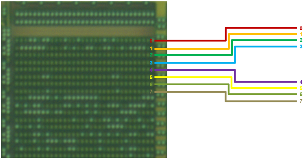
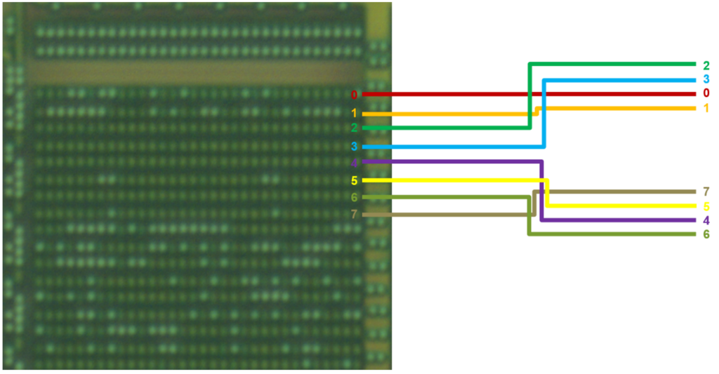
Figure 1. Normal (unscrambled) output
Figure 2. Scrambled output

The ordering may also vary byte-to-byte, making reverse engineering more difficult.

Is the ROM encrypted?

Encryption is far more difficult to reverse engineer because the data is routed out of the memory and into the CPU logic, which is usually vast and, on its face, random. The data will be routed to the decryption circuitry, which may only be a few dozen logic cells.

Finding the decryption circuitry in a sea of one hundred thousand logic cells with no direction on where to start is an extremely difficult task. It may be necessary to reverse engineer the entire CPU logic; however, there are isolation techniques like thermal or photon emission that can help identify a specific area of interest on the chip. Using such techniques, the chip is instructed to repeatedly decrypt data while the entire chip is monitored for heat or light emissions, revealing the area of the chip that is performing the decryption. This smaller area of the chip then becomes the focus of reverse engineering.

Is the ROM both scrambled and encrypted?

If the ROM is both scrambled and encrypted, recovering the data will require analysis of the addressing logic and reverse engineering some if not all of the CPU logic. If the raw data is encrypted, the physical bit pattern will look the same, whether it is scrambled or not.

How do you deprocess a chip?

Deprocessing is the physical removal of layers from a finished chip using chemical and mechanical techniques. The process is necessarily destructive and can be used to remove one or more layers, depending on the target.

Consider the following example chip:
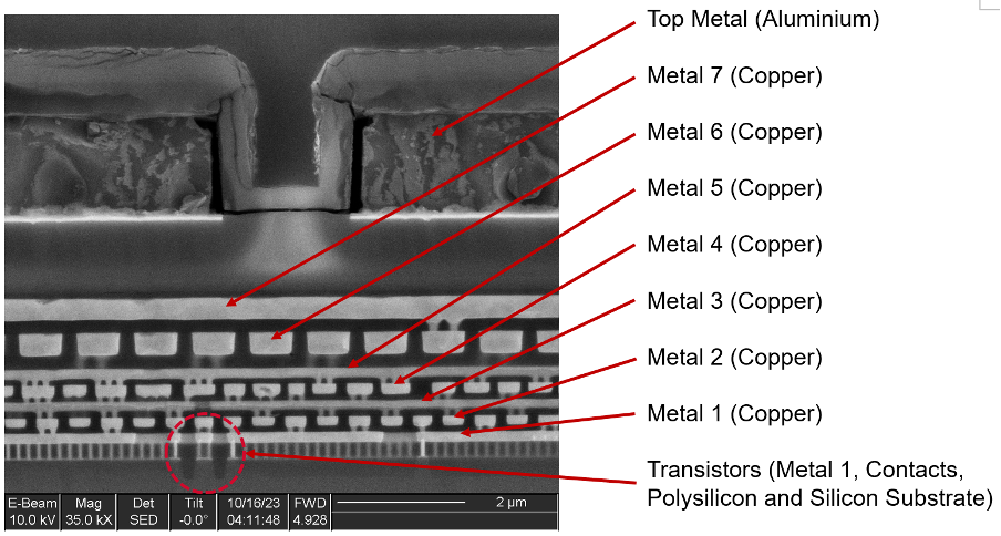
Figure 3. Example chip cross-section showing metal layers and transistors

We can see that the chip is constructed of many layers of copper circuitry, all embedded in an insulator (glass-type material). Transistors are literally the building blocks of digital components and are fabricated on the silicon substrate at the bottom of the chip. Therefore, the ROM transistors will be located on the bottom as well. The raw bits we are looking for (the ROM encoding layer) will likely be at the Contact, Metal 1, or Via 1 layer (between Metal 1 and Metal 2), but we won’t know for sure until we start destroying some chips.

If we have the time and sufficient samples, we can start by removing all of the layers from one chip in order to analyze the floorplan. Based on this analysis, we can map out where the memories are located and even identify what types of memories are present, such as Flash, SRAM, DRAM, or ROM. This will help identify the specific area of the chip to focus on when attempting to extract the raw bits. In addition, we could also cross-section a chip at the location of the ROM to help determine which layer contains the bit encoding to guide our work.

If we don’t have the time or the samples, we can just go ahead and carefully deprocess a single chip, and at some point, the ROM bits will appear. But if we deprocess too far, we will go past the bit encoding layer and lose the data.

For our work, we will use the most basic and fastest technique—mechanical polishing. While many argue that mechanical polishing is the most effective method for deprocessing chips, it is also the most skill dependent.

We can polish in several ways (in order of increasing sophistication and cost):

  1. Manual finger polishing: The decapsulated chip is placed on the fingertip and polished on a static plate or piece of glass.
  2. Turntable finger polishing: Similar to manual but uses a rotating platen to expedite the polishing process (and eliminate Repetitive Strain Injury!).
  3. Manual polishing with fixture (jig): Uses a rotating platen in conjunction with a polishing fixture that can be adjusted to compensate for non-planarity.
  4. Semi-automated polishing: Uses a purpose-built system with control over:
    1. Platen speed
    1. Sample planarity
    1. Force applied to sample
    1. Sample rotation (in addition to platen rotation)

In this example we used the third approach because a turntable accelerates progress, and a polishing jig offers fine angle control. Additionally, the manual polishing table and jig, as well as the abrasives involved, are relatively low-cost items, keeping the approach within reach of a skilled and motivated hobbyist.
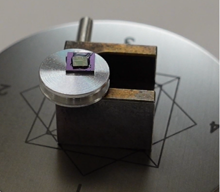
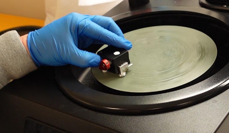
Figure 4. A decapsulated chip mounted to the polishing stub
Figure 5. The stub attached to the polishing jig while being polished

Determining when to stop polishing (end pointing) is difficult; however, when we hit the ROM encoding layer, we should see some kind of pattern under an optical microscope, even at 5x magnification.

The image below was taken at 20x magnification, and we can categorically say that we have reached the right layer.
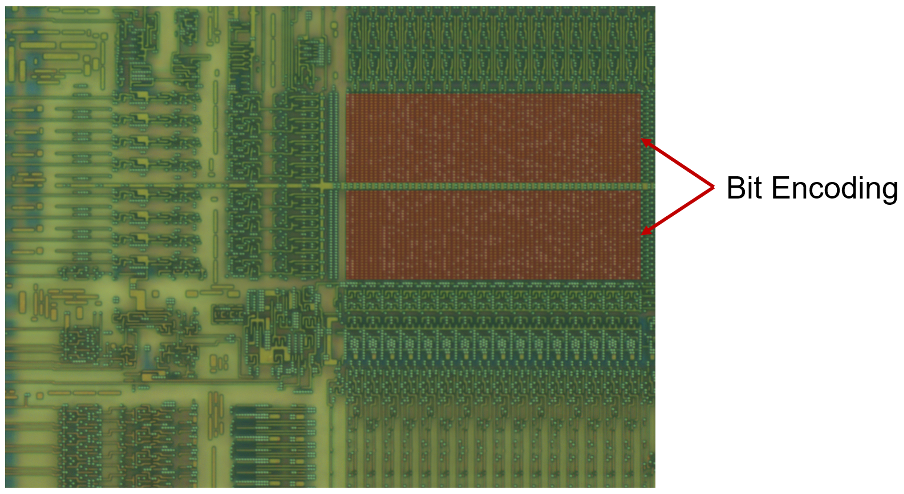
Figure 6. Corner of ROM exposed at bit encoding layer

The bits appear as white dots from above, because they are bullet-shaped Tungsten interconnects, a little like the contacts shown in the following cross-section images:
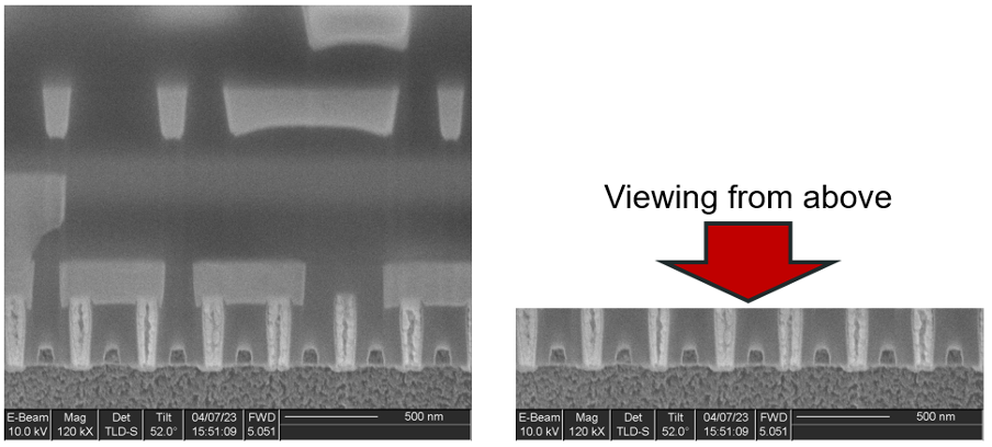
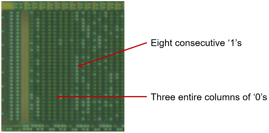
Figure 7. ROM cross-section fully processed (left) and deprocessed to the bit encoding layer (right)
Figure 8. Sample area for initial visual inspection

We can see from a very high-level visual inspection that the ROM cannot possibly be encrypted, due to the distribution of ones versus zeroes. If the data was properly encrypted, then the distribution would appear random; however, a visual assessment is sufficient to confirm a lack of entropy without the need to formally calculate[1] it with binwalk[2] or another tool. We can conclude that although the data may be scrambled, it is not encrypted. There is enough evidence to tell us that if we extract the raw bits, we can derive the addressing to then get us back to an understandable binary.

For now, we don’t need to carefully analyze the addressing circuit; all we need is to determine if there is any scrambling in the addressing logic. We can do this visually.
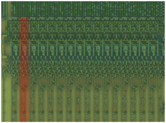
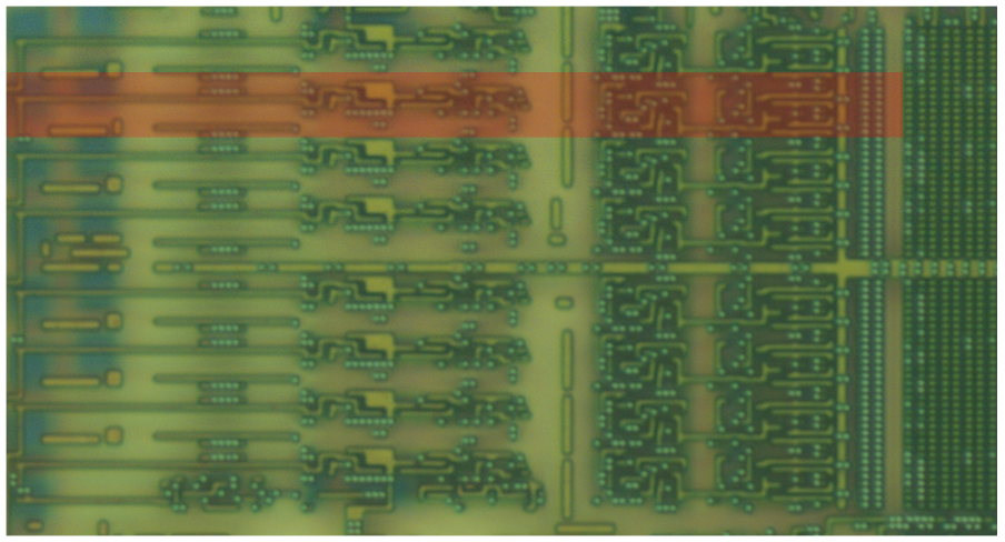
Figure 9. Sample area of decoding/addressing circuit (bottom)
Figure 10. Sample area of decoding/addressing circuit (left)
Figure 11 Sample area of decoding/addressing circuit (between blocks)

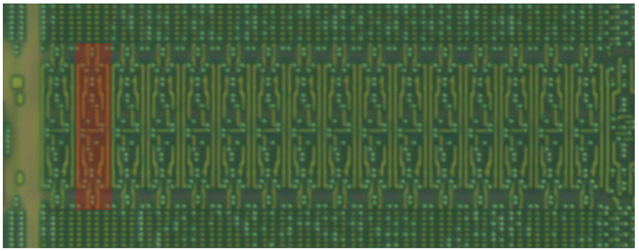
When we isolate a small area of the decoding/addressing circuitry at any point (bottom, left, or between the blocks), it is perfectly repeated. This proves that the ROM is not scrambled, and all we need to do is to work out how the bits are read to recreate the full binary. That, and extract the raw bits, of course.

No Scrambling 😊

No Encryption 😊

How do you extract the raw bits?

It is preferable that we automate the extraction process, as the ROM’s capacity is 16 KB (128,000 single bits), which is far too much to extract manually. First, we must determine if our optical images are good enough to reliably extract the raw bits. If not, we may need to use a Scanning Electron Microscope (SEM) to obtain higher resolution, higher contrast images.
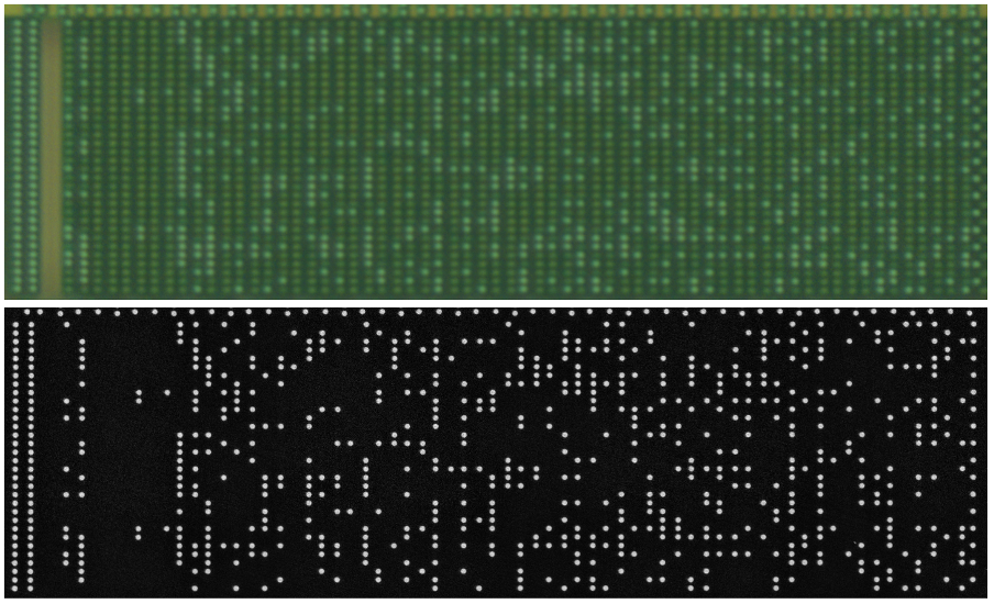
Figure 12. Sample area of raw bits imaged optically (top) and by SEM (bottom)

Clearly there is a huge difference in resolution and, more importantly, contrast between the two types of images. It’s obvious that using SEM images would expedite the extraction process, but let’s see if we can use the optical images and do this on a shoestring budget.

First, we need to optimize the optical test image with photo editing software to maximize our chances of success. A good start is always to use the filters in Photoshop such as ‘Noise – Despeckle’ and ‘Noise – Dust and Scratches.’ The final step would be to manipulate the levels to maximize the contrast.
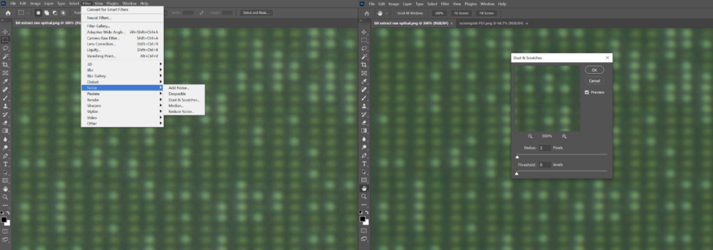
Figure 13. Screenshots showing Adobe Photoshop noise filters being applied
Figure 14. Sample area of raw bits imaged optically and filtered/optimized

Perhaps quite surprisingly, simply by filtering and adjusting the levels of the optical image, we can almost end up with the same result as with the SEM.
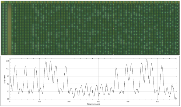
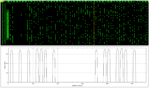
Figure 15. Plot of unfiltered optical image
Figure 16. Plot of filtered optical image

From this simple test, we can conclude that any effective tool will be capable of reliably extracting the raw bits from our optical images.

Figure 17. Single block with bit extraction grid overlaid
Figure 18. Zoomed view of bits with extraction grid overlaid

Commercial software is available for semi-automated ROM bit extraction. The software measures the brightness of the area around the line intersections and compares that against a user-defined estimate for both a one and a zero. The software then assigns values to each area in which a bit exists, then exports the values to a text file. Below is the text extracted from this small piece of ROM. This is a fraction of one of 64 sections within the memory array, so some time is required for a full extraction. There is certainly an AI/ML opportunity here to expedite the process.
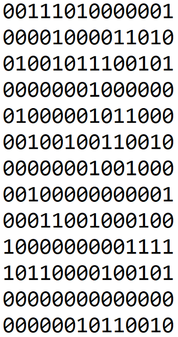
After repeating the process many times, we have the entire ROM in our hands, and we can move onto the next step: deriving how the bits are addressed. At this point, we will have a usable binary to work with in IDA Pro or Binary Ninja so we can understand the boot process and find some potential areas of weakness we can glitch.

Bits to Binary

As this is a chip with a known vulnerability, it was possible to dump the entire ROM via JTAG. We will use this dump to help us do two things:

  1. Deduce how the ROM is addressed
  2. Compare our physically extracted ROM with the JTAG dump to validate our process

To illustrate the analysis of our physically extracted dump, we will use the higher-resolution SEM images we acquired after the optical images were taken.

Let’s start by looking at the electrical dump of the ROM. The following output is the beginning and end of the ROM .bin, with the end looking very much like a checksum. We know this is commonly used by this manufacturer, so after many zero bytes, there are two bytes of data at the very end of the file.
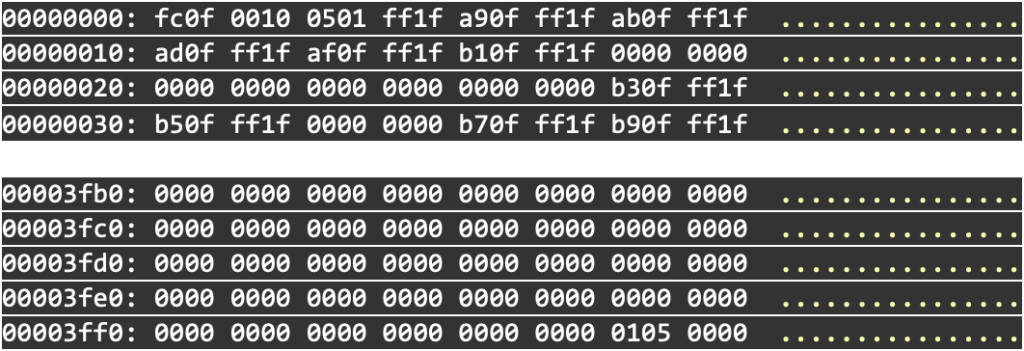
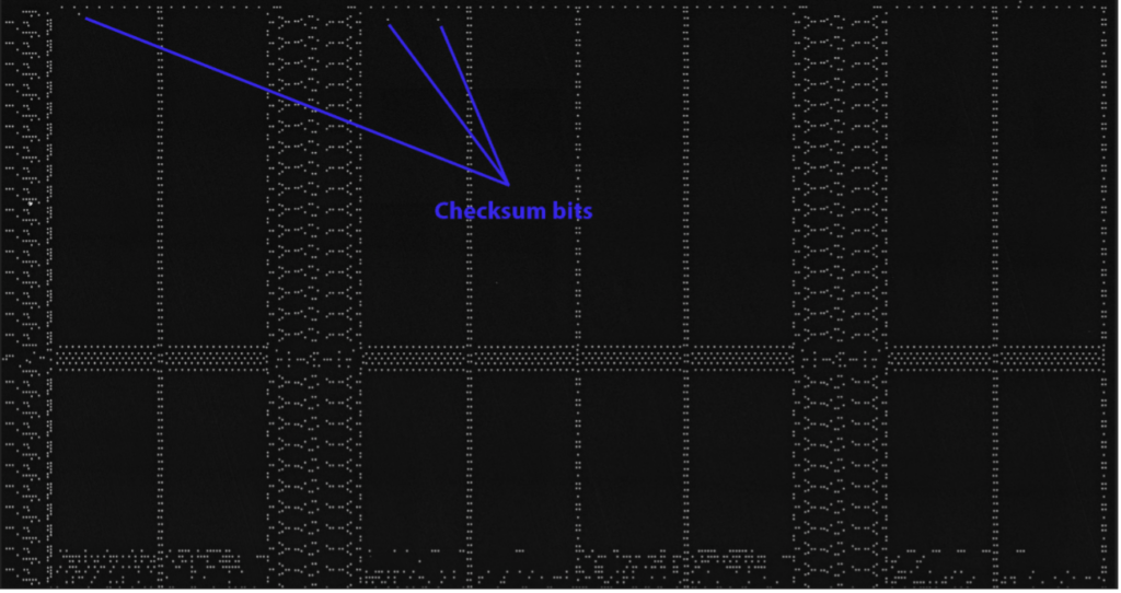
Figure 19. Hex dump output of the start (top) and end (bottom) of the ROM .bin
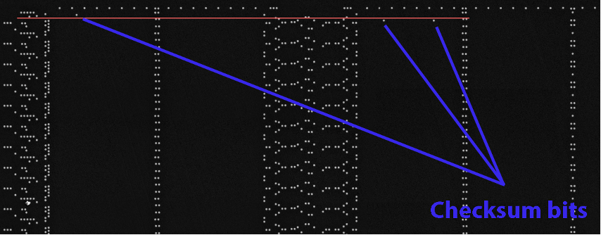
Figure 20. Bottom section of ROM SEM stitch with checksum bits annotated
Figure 21. Close-up showing that the three bits are not in the same row. One on the first row, then two on the second row (the red line is perfectly parallel)

From the fact that we have the two-byte checksum (0105) in hex, and that the corresponding raw bits (0000 0001 0000 0101) are not in a linear pattern, then we must assume that there is some flipping/mirroring happening on the bit addressing. The fact that the bits are split over two rows also gives us a clue.

Now our checksum is beginning to make sense. With a checksum of 0105 (0000 0001 0000 0101), there must only be one way to read it. Essentially, we are looking for how the three ones are addressed.

First, we can see that the three bits are all on the same bit column, so we can ignore the rest. It makes things easier to visualize by annotating all of the bit columns, then highlighting the only column (column 0) we care about in yellow. The values are now much easier to read by eye, and we can see the direction in which they are read by the memory array.
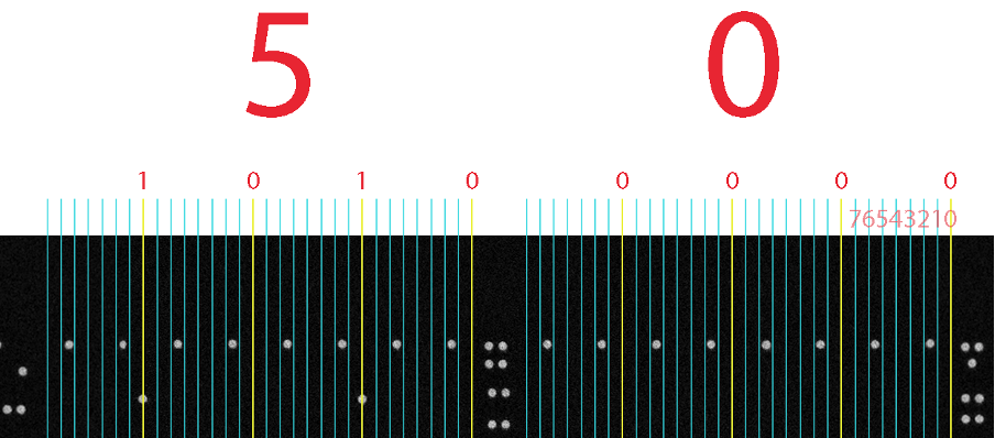
Figure 22. Right side of checksum area annotated with columns, binary values, and hex
Figure 23. Entire width of checksum area annotated with columns, binary values, and hex

We now see that 0105, albeit not in a logical order for a human. There is one question mark remaining: Do we assume that we read the left side in reverse first (01) followed by the second (05)? There we have a simple 50% chance of being correct, and to find out, we can apply that to the more densely populated areas of ROM.
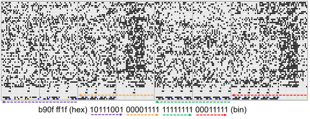
Figure 24. Opposite end of ROM annotated with read order, binary values, and corresponding hex

The portion of ROM above shows the hex value along with the raw binary for the two-word width of the ROM array. The colored arrows illustrate the direction in which the bits are read from the .bin and how they are read from the raw bit image. The following is a closer view of one byte, where blue bits are logical ones and yellows are logical zeros:
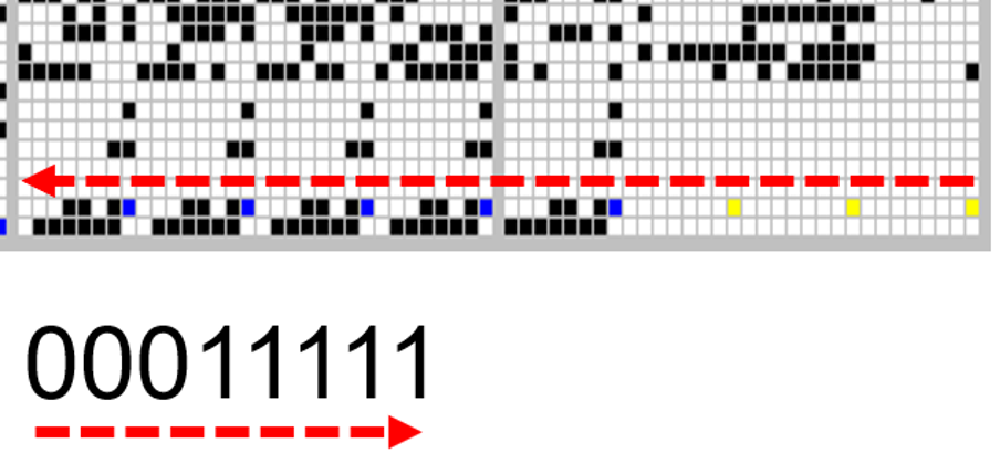
the end of the ROM, annotated with read order and binary values

Finally, a binary!!!

The following image contains some dumped bytes from the target. This can be later be opened in the reversing tool of our choice, and after some preparation work, we can begin reverse engineering and identifying the potential weaknesses. In this case, as some readers might know, the target sample has a known vulnerability that can be exploited via fault injection. This vulnerability can allow an attacker with physical access to the device to retrieve the entire contents, even if the chip has been locked down.

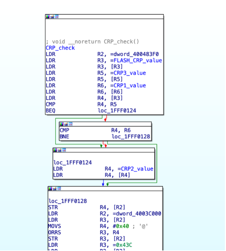
Figure 26. Some bytes dumped from the target chip
Figure 27. Part of the boot process where CRP values are read and are controlling access to the debugging interfaces

Overall Conclusions

  • While a chip with a known vulnerability was used in this case study for comparative purposes, the same techniques can be applied to a chip without this vulnerability
  • The electrical version of the ROM dump matched 100% with the physically extracted version
  • Physical ROM bit extraction is skill-dependent, but can be carried out using a relatively basic toolset such as:
    • Basic polishing turntable
    • Handheld polishing jig
    • Diamond abrasives
    • Optical microscope
  • ROM binary extraction is dependent on:
    • Existence of encryption
    • Complexity of scrambling
    • Patience!
  • ROM binary analysis and isolation of glitching/fault injection points is possible
  • Electrical and electromagnetic fault injection techniques are skill- and chip-dependent; however, the bar of entry is relatively low (hundreds to thousands of dollars)

[1] https://resources.infosecinstitute.com/topics/cryptography/entropy-calculations/
[2] https://github.com/ReFirmLabs/binwalk

INSIGHTS, RESEARCH | April 17, 2024

Accessory Authentication – part 3/3

This is Part 3 of a 3-Part series. You can find Part 1 here and Part 2 here.

Introduction

In this post, we continue our deep dive comparison of the security processors used on a consumer product and an unlicensed clone. Our focus here will be identifying and characterizing memory arrays.

Given a suitably deprocessed sample, memories can often be recognized as such under low magnification because of their smooth, regular appearance with distinct row/address decode logic on the perimeter, as compared to analog circuitry (which contains many large elements, such as capacitors and inductors) or autorouted digital logic (fine-grained, irregular structure).

Identifying memories and classifying them as to type, allows the analyst to determine which ones may contain data relevant to system security and assess the difficulty and complexity of extracting their content.

OEM Component

Initial low-magnification imaging of the OEM secure element identified 13 structures with a uniform, regular appearance consistent with memory.

Higher magnification imaging resulted in three of these structures being reclassified as non-memory (two as logic and one as analog), leaving 10 actual memories.

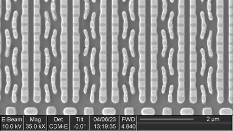
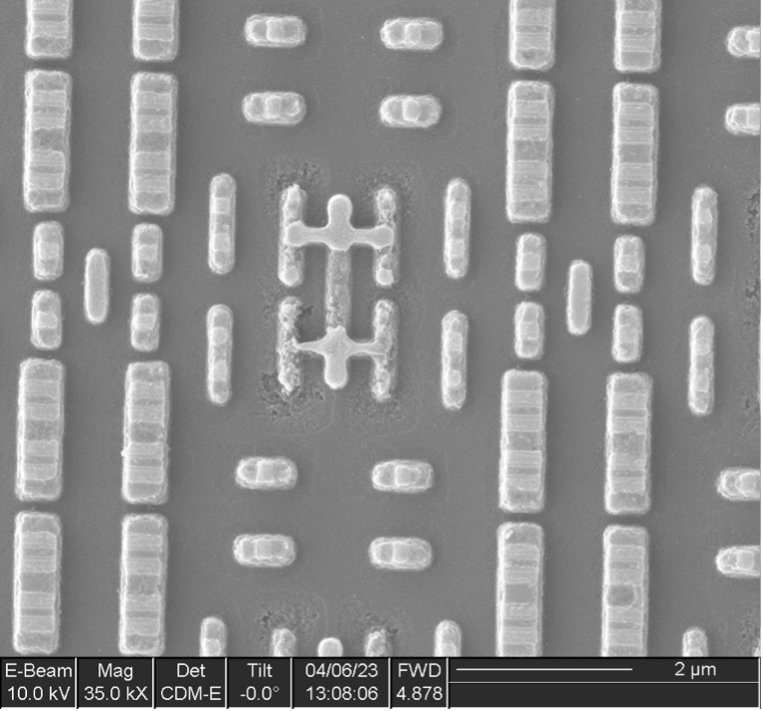
Figure 1. Logic circuitry initially labeled as memory due to its regular structure
Figure 2. Large capacitor in analog block

Of the remaining 10 memories, five distinct bit cell structures were identified:

  • Single-port (6T) SRAM
  • Dual-port (8T) SRAM
  • Mask ROM
  • 3T antifuse
  • Floating gate NOR flash

Single-port SRAM

13 instances of this IP were found in various sized arrays, with capacities ranging from 20 bits x 8 rows to 130 bits x 128 rows.

Some of these memories include extra columns, which appear to be intended as spares for remapping bad columns. This is a common practice in the semiconductor industry to improve yield: memories typically cover a significant fraction of the die surface and thus are responsible for a large fraction of manufacturing defects. If the device can remain operable despite a defect in a memory array, the overall yield of usable chips will be higher.

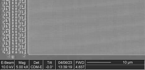
Figure 3. Substrate overview of a single-port SRAM array
Figure 4. Substrate closeup view of single-port SRAM bit cells

Dual-port SRAM

Six instances of this IP were found, each containing 320 bit cells (40 bytes).

Figure 5. Dual-port SRAM cells containing eight transistors

Mask ROM

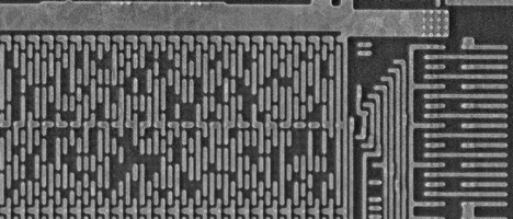
Two instances of this IP were found, with capacities of 256 Kbits and 320 Kbits respectively. No data was visible in a substrate view of the array.

Figure 6. Substrate view of mask ROM showing no data visible

A cross section (Figure 7) showed irregular metal 1 patterns as well as contacts that did not go to any wires on metal 1, strongly suggesting this was a metal 1 programmed ROM. A plan view of metal 1 (Figure 8) confirms this. The metal 1 pattern also shows that the transistors are connected in series strings of 8 bits (with each transistor in the string either shorted by metal or not, in order to encode a logic 0 or 1 value), completing the classification of this memory as a metal 1 programmed NAND ROM.

Figure 7. Cross section of metal 1 programmed NAND ROM showing irregular metal patterns and via with unconnected top
Figure 8. Top-right corner of one ROM showing data bits and partial address decode logic

IOActive successfully extracted the contents of both ROMs and determined that they were encrypted. Further reverse engineering would be necessary to locate the decryption circuitry in order to make use of the dumps.

Antifuse

Five instances of this IP were found, four with a capacity of 4 rows x 32 bits (128 bits) and one with a capacity of 32 rows x 64 bits (2048 bits).

The bit cells consist of three transistors (two in series and one separate) and likely function by gate dielectric breakdown: during programming, high voltage applied between a MOSFET gate and the channel causes the dielectric to rupture, creating a short circuit between the drain and gate terminals.

Antifuse memory is one-time programmable and is expensive due to the very low density (significantly larger bit cell compared to flash or ROM); however, it offers some additional security because the ruptured dielectric is too thin to see in a top-down view of the array, rendering it difficult to extract the contents of the bit cells. It is also commonly used for small memories when the complexity and re-programmability of flash memory is unnecessary, such as for storing trim values for analog blocks or remapping data for repairing manufacturing defects in SRAM arrays.

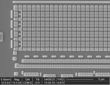
Figure 9. Antifuse array
Figure 10. Cross section of antifuse bit cells

Flash

A single instance of this IP was found, with a capacity of 1520 Kbits.

This memory uses floating-gate bit cells connected in a NOR topology, as is common for embedded flash memories on microcontrollers.

Figure 11. Substrate plan view of bit cells
Figure 12. Cross section of NOR Flash memory

Clone Component

Floorplan Overview

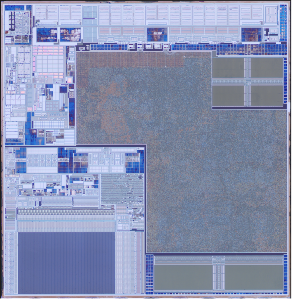
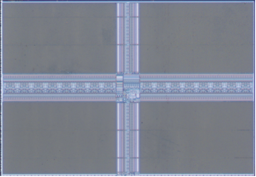
Figure 13. Substrate view of clone secure element after removal of metal and polysilicon

The secure element from the clone device contains three obvious memories, located at the top right, bottom left, and bottom right corners.

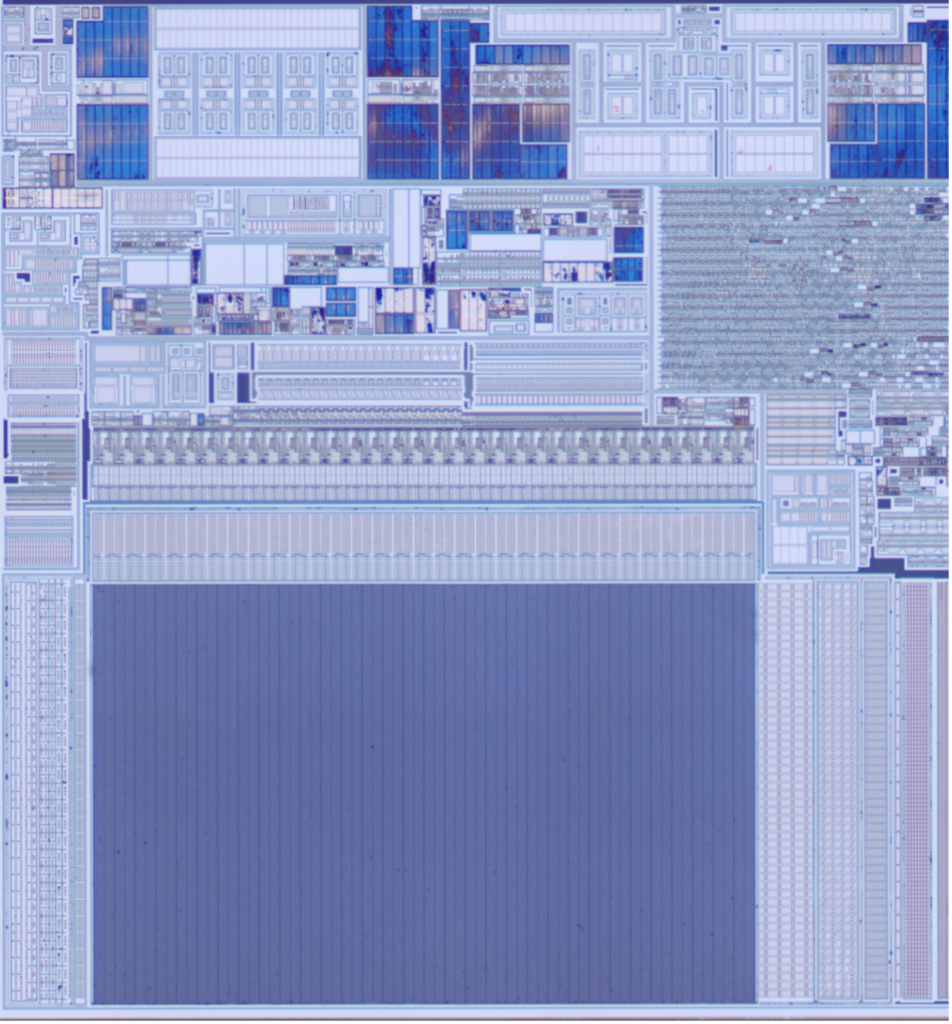
Lower-left Memory

The lower-left memory consists of a bit cell array with addressing logic at the top, left, and right sides. Looking closely, it appears to be part of a larger rectangular block that contains a large region of analog circuitry above the memory, as well as a small amount of digital logic.

This is consistent with the memory being some sort of flash (likely the primary code and data storage for the processor). The large analog block is probably the high voltage generation for the program/erase circuitry, while the small digital block likely controls timing of program/erase operations.  

The array appears to be structured as 32 bits (plus 2 dummy or ECC columns) x 64 blocks wide, by 2 bits * 202 rows (likely 192 + 2 dummy features + 8 spare). This gives an estimated usable array capacity of 786432 bits (98304 bytes, 96kB).

Figure 14. Overview of bottom left (flash) memory
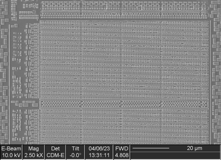
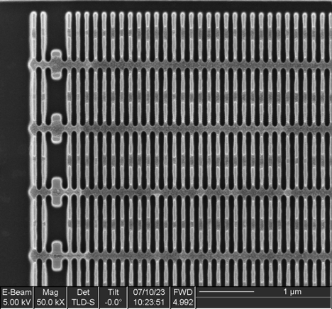
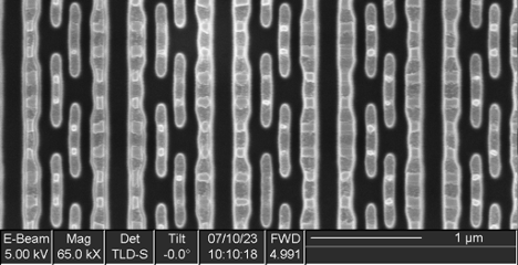
Figure 15. SEM substrate image of flash memory

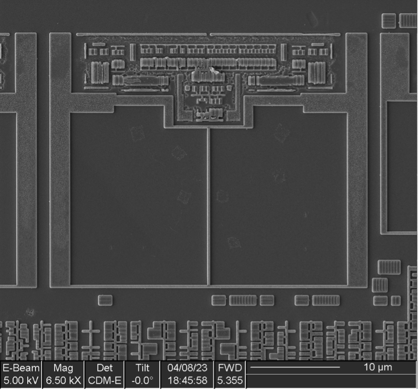
A cross section was taken, which did not show floating gates (as compared to the OEM component). This suggests that this component is likely using a SONOS bit cell or similar charge-trapping technology.

Lower-right Memory

The lower-right memory consists of two identical blocks side-by-side, mirrored left-to-right. Each block consists of 128 columns x 64 cells x 3 blocks high, for a total capacity of 49152 bits (6144 bits, 6 kB).

Figure 16. Lower-right memory

At higher magnification, we can see that the individual bit cells consist of eight transistors, indicative of dual-port SRAM—perhaps some sort of cache or register file.

Figure 17. Dual-port SRAM on clone secure element (substrate)
Figure 18. Dual-port SRAM on clone secure element (metal 1)

Upper-right Memory

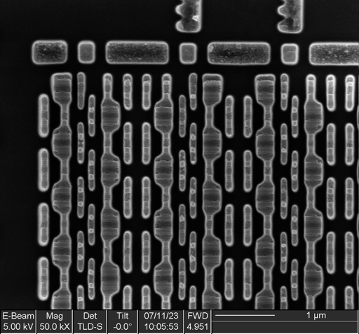
The upper – right memory consists of a 2 x 2 grid of identical tiles, each 128 columns x 160 rows (total capacity 81920 bits/10240 bytes/10 kB).

Figure 19. Upper-right SRAM array

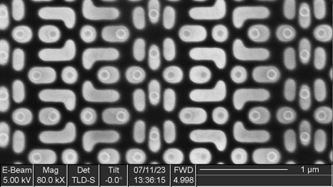
Upon closer inspection, the bit cell consists of six transistors arranged in a classic single-port SRAM structure.

Figure 20. SEM substrate image of 6T SRAM cells
Figure 21. SEM metal 1 image of 6T SRAM cells

Concluding Remarks

The OEM component contains two more memory types (mask ROM and antifuse) than the clone component. It has double the flash memory and nearly triple the persistent storage (combined mask ROM and flash) capacity of the clone, but slightly less SRAM.

Overall, the memory technology of the clone component is significantly simpler and lower cost.

Overall Conclusions

OEMs secure their accessory markets for the following reasons:

  • To ensure an optimal user experience for their customers
  • To maintain the integrity of their platform
  • To secure their customers’ personal data
  • To secure revenue from accessory sales

OEMs routinely use security chips to protect their platforms and accessories; cost is an issue for OEMs when securing their platforms, which potentially can lead to their security being compromised.

Third-party solution providers, on the other hand:

  • Invest in their own labs and expertise to extract the IP necessary to make compatible solutions
  • Employ varied attack vectors with barriers of entry ranging from non-invasive toolsets at a cost of $1,000 up, to an invasive, transistor-level Silicon Lab at a cost of several million dollars
  • Often also incorporate a security chip to secure their own solutions, and to in turn lock out their competitors
  • Aim to hack the platform and have the third-party accessory market to themselves for as long as possible
INSIGHTS, RESEARCH |

Accessory Authentication – part 2/3

This is Part 2 of a 3-Part series. You can find Part 1 here and Part 3 here.

Introduction

In this post, we continue our deep dive comparison of the security processors used on a consumer product and an unlicensed clone. Our focus here will be comparing manufacturing process technology.

We already know the sizes of both dies, so given the gate density (which can be roughly estimated from the technology node or measured directly by locating and measuring a 2-input NAND gate) it’s possible to get a rough estimate for gate count. This, as well as the number of metal layers, can be used as metrics for overall device complexity and thus difficulty of reverse engineering.

For a more accurate view of device complexity, we can perform some preliminary floorplan analysis of each device and estimate the portions of die area occupied by:

  • Analog logic (generally uninteresting)
  • Digital logic (useful for gate count estimates)
  • RAM (generally uninteresting aside from estimating total bit capacity)
  • ROM/flash (allows estimating capacity and, potentially, difficulty of extraction)

OEM Component

We’ll start with the OEM secure element and take a few cross sections using our dual-beam scanning electron microscope/focused ion beam (SEM/FIB). This instrument provides imaging, material removal, and material deposition capabilities at the nanoscale.

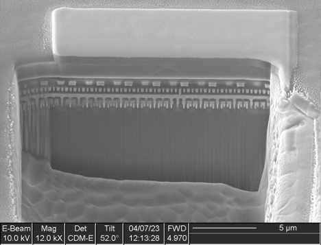
Figure 1. SEM image showing FIB cross section of OEM component

To cross section a device, the analyst begins by using deposition gases to create a protective metal cap over the top of the region of interest. This protects the top surface from damage or contamination during the sectioning process. This is then followed by using the ion beam to make a rough cut a short distance away from the region of interest, then a finer cut to the exact location. The sample can then be imaged using the electron beam.

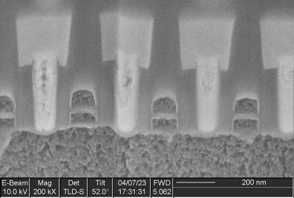
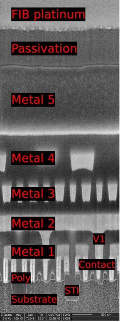
Figure 1 shows a large rectangular hole cut into the specimen, with the platinum cap at top center protecting the surface. Looking at the cut face, many layers of the device are visible. Upon closer inspection (Figure 2), we can see that this device has four copper interconnect layers followed by a fifth layer of aluminum.

Figure 2. Cross section with layers labeled
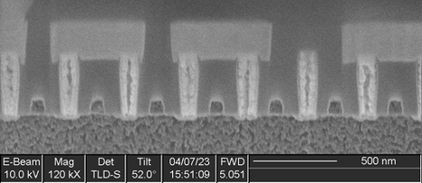
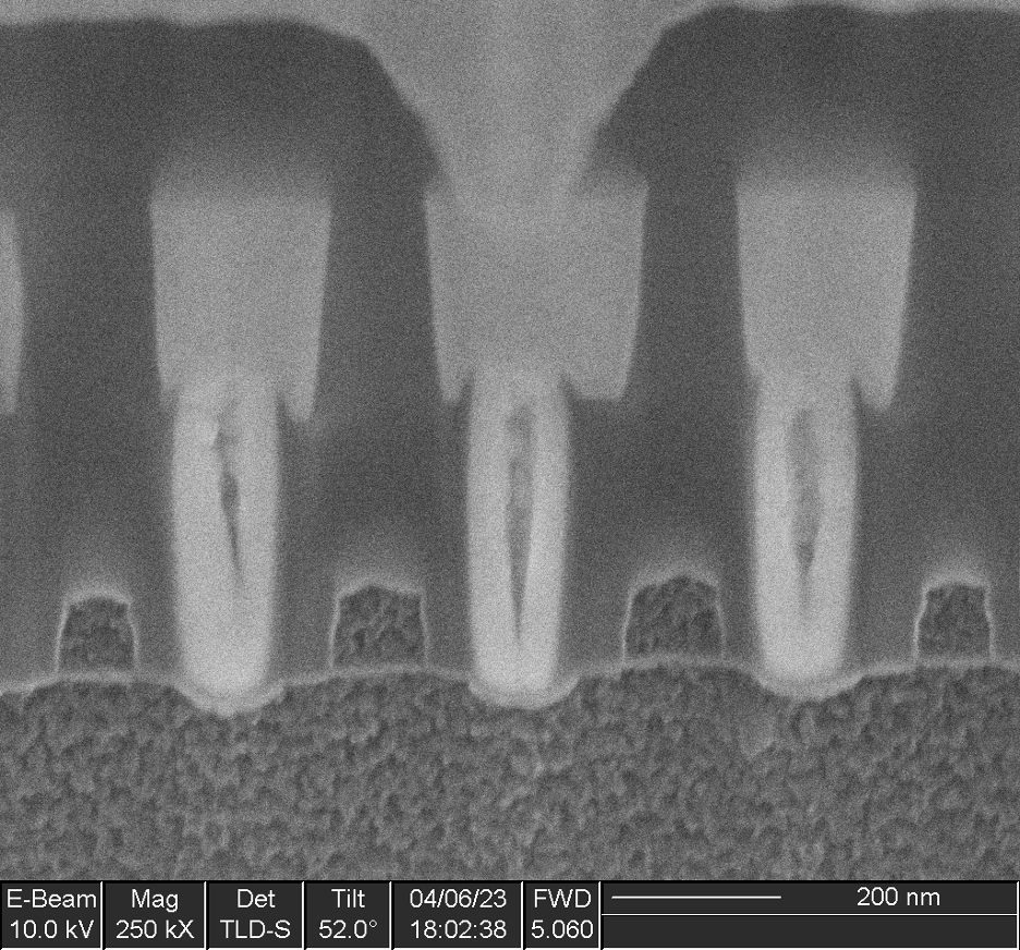
Figure 3. Cross-section view of OEM component showing individual transistor channels

At higher magnification (Figure 3), we can clearly see individual transistors. The silicon substrate of the device (bottom) has been etched to enhance contrast, giving it a rough appearance. The polysilicon transistor gates, seen end-on, appear as squares sitting on the substrate. The bright white pillars between the gates are tungsten contacts, connecting the source and drain terminals of each transistor to the copper interconnect above.

Figure 4. 6T SRAM bit cells on OEM component

Based on measurements of the gates, we conclude that this device is made on a 90 nm technology:

  • Contacted gate pitch: 282 nm
  • M1 pitch: 277 nm
  • 6T SRAM bit cell (Figure 4): 1470 x 660 nm (0.97 µm2)

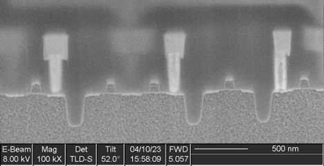
We can also use cross sections to distinguish between various types of memory. Figure 5 is a cross section of one of the memory arrays of the OEM device, showing a distinctive double-layered structure instead of the single polysilicon gates seen in Figure 3. This is a “floating gate” nonvolatile memory element; the upper control gate is energized to select the cell while the lower floating gate stores charge, representing a single bit of memory data.

The presence of metal contacts at both sides of each floating gate transistor (rather than at either end of a string of many bits) allows us to complete the classification of this memory as NOR flash, rather than NAND.

Figure 5. Cross section of NOR flash memory on OEM component showing floating gates

The overall device is approximately 2400 x 1425 µm (3.42 mm2), broken down as:

  • 67% (2.29 mm2): memories and analog IP blocks
  • 33% (1.13 mm2): standard cell digital logic

Multiplying the logic area by an average of published cell library density figures for the 90nm node results in an estimated 475K gates of digital logic (assuming 100% density) for the OEM security processor. The actual gate count will be less than this estimate as there are some dummy/filler cells in less dense areas of the device.

Clone Component

Performing a similar analysis on the clone secure element, we see five copper and one aluminum metal layers (Figure 6).

Figure 6. Cross section of clone security processor showing layers
Figure 7. Closeup of SRAM transistors from clone security processor

Interestingly, the clone secure element is made on a more modern process node than the OEM component:

  • Contacted gate pitch: 225 nm
  • Minimum poly pitch: 158 nm
  • SRAM bit cell: 950 x 465 nm (0.45 µm2)

The transistor gates appear to still be polysilicon rather than metal.

Figure 8. NAND2 cell from clone component, substrate view with metal and polysilicon removed

These values are in-between those reported for the 65 nm and 45 nm nodes, suggesting this device is made on a 55 nm technology. The lack of metal gates (which many foundries began using at the 45 nm node) further reinforces this conclusion.

The overall device is approximately 1190 x 1150 µm (1.36 mm2), broken down as:

  • 37% (0.50 mm2): memories
  • 27% (0.36 mm2): analog blocks and bond pads
  • 31% (0.42 mm2): standard cell digital logic
  • 5% (0.07 mm2): filler cells, seal ring, and other non-functional areas

Given the roughly 0.42 mm2 of logic and measured NAND2 cell size of 717 x 1280 nm (0.92 µm2 or 1.08M gates/mm2 at 100% utilization), we estimate a total gate count of no more than 450K—slightly smaller than the OEM secure element. The actual number is likely quite a bit less than this, as a significant percentage (higher than on the OEM part) of the logic area is occupied by dummy/filler cells.

In part 3, we continue our deep dive comparison of the security processors used on a consumer product and an unlicensed clone. There we will focus on identifying and characterizing the memory arrays.