INSIGHTS | December 5, 2009

Volunteers to help cleanup WordPress problems?

Whenever the blog is enabled, spammers are able to deface the main pages index.html file replacing it with hundreds of spam links to software.

The only way we can stop it is to stop the blog. We’ve tried cleaning the blog up but they still get in somehow through WordPress :(.

If you think you can help us, please email tech at flylogic.net

Thanks!

RESEARCH | January 8, 2009

Intel 4004

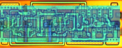
Before going deeper into the analysis of today’s chips, we will take a quick journey to where it all began: the Intel 4004, world’s first widely-used microprocessor. The 4004 and most other antiquated chips differ from modern chips in two main characteristics: They only use a single type of transistor (PMOS or NMOS) and each logic gate is custom-designed to best utilize the available area — an inevitable optimization for chips built from transistors about 150x larger than those used in their modern descendants.

Each of the gates is composed of two transistors and one resistor. If either of the transistors is open (that is: having Vcc applied to its gate), the output is strongly connected to Vcc. If neither of the transistors is open, the gate is weakly connected to GND through the resistor, but still strong enough to pull the output to GND.

PMOS is very area-efficient, but more power hungry and slower than alternatives such as CMOS, which combines PMOS and NMOS transistors as illustrated in this post. It’s beautiful to see how none of the inefficiencies we see in modern chips are found on the 4004 and how the available space is completely filled with logic.

As a challenge for next time, identify the extra 3 layers that the Intel museum claims. Last episode’s challenge was correctly solved first by Jeri Ellsworth. Respect for her almost perfect circuit diagram as well as her remarkable on-your-kitchen-table semiconductors fab.

Credit for the chips go to Tim McNerney. Tim is an expert on the 4004 who has built an interactive exhibit of the chip for the Intel museum. For more information please visit the Intel 4004 35th anniversary project web site.

-Karsten Nohl

INSIGHTS | September 13, 2008

Reverse-Engineering Custom Logic (Part 1)

Today we are taking you one step deeper into a microchip than we usually go. We look at transistors and the logic functions they compose, which helps us understand custom ASICs now found in some secured processors.

To reverse-engineer the secret functionality of an ASIC, we identify logic blocks, map out the wiring between the blocks, and reconstruct the circuit diagram. Today, we’ll only be looking at the first step: reading logic. And we start with the easiest example of a logic function: the inverter.

To read logic, you first have to find the transistors and decide where Vcc (+) and ground (-) are located. Transistors are easy to spot. They will always look very similar to those two transistors marked in the picture: A rectangle shape with a line in the middle. Vcc is always next to the larger transistors (PMOS) and ground is closer to the smaller ones (NMOS).

Once you identified the transistors, you draw a small circuit diagram that shows how they are connected to each other. In the example, the inputs of the two transistors are connected and so are their outputs on the left side. From this circuit diagram you can read that whatever you assert at the input, the output will be forced to the opposite state — an inverter.

Every gate will follow these basic principles, but vary in the number and constellation of transistors. A 2-NOR gate (Y = !(A|B) ), for instance, is composed of 4 transistors in this setup:

Once you figured out a gate, you can recognize every occurrence of that function on the whole chip because the exact same shape is always used for the same function. Generally, you only need to read a few dozens gates at most to generate a map of functions across whole chip. Get a head start on reading logic and check out the logic gate collection at The Silicon Zoo.

Here is a challenge for you to try (open in GIMP or Photoshop and toggle between the different layers):

It’s about the hardest function found on most chips with a total of 34 transistors, 3 inputs, 2 outputs, and time-variant behavior. The solution will be posted next week.
INSIGHTS |

New Author: Herr Karsten Nohl!

We are proud to announce that those who enjoy reading the blog (which we apologize for the lack of content lately) can soon enjoy reading posts from Karsten Nohl as well.

For those of you who are not familiar with Karsten, he played an important role in the discovery and analysis of the Crypto-1 mathematical algorithm found in Philips (NXP) Mifare RFID devices.

He recently obtained his PhD from University of Virginia in the United States.   He’s well known within the Chaos Computer Club (CCC) in Germany as well.

We too look forward to reading Karsten’s posts.   Feel free to give Karsten a round of applause by posting a quick comment!

Karsten- Congratulations on your PhD!!