INSIGHTS, RESEARCH | May 16, 2024

Field-Programmable Chips (FPGAs) in Critical Applications – What are the Risks?

What is an FPGA?

Field-Programmable Gate Arrays (FPGAs) are a type of Integrated Circuit (IC) that can be programmed or reprogrammed after manufacturing. They consist of an array of logic blocks and interconnects that can be configured to perform various digital functions. FPGAs are commonly used in applications where flexibility, speed, and parallel processing capabilities are required, such as telecommunications, automotive, aerospace, and industrial sectors.

FPGAs are often found in products that are low volume or demand short turnaround time because they can be purchased off the shelf and programmed as needed without the setup and manufacturing costs and long lead times associated with Application-Specific Integrated Circuits (ASICs). FPGAs are also popular for military and aerospace applications due to the long lifespan of such hardware as compared to typical consumer electronics. The ability to update deployed systems to meet new mission requirements or implement new cryptographic algorithms—without replacing expensive hardware—is valuable.

These benefits come at a cost, however: additional hardware is required to enable reprogramming. An FPGA-based design will use many more transistors than the same design implemented as an ASIC, increasing power consumption and per-device costs.

Implementing a circuit with an FPGA vs an ASIC can also come with security concerns. FPGA designs are compiled to a “bitstream,” a digital representation of the circuit netlist, which must be loaded into the FPGA for it to function. While bitstream formats are generally undocumented by the manufacturer, several projects are working towards open-source toolchains (e.g., Project X-Ray for the Xilinx 7 series) and have reverse engineered the bitstream formats for various devices.

FPGA bitstreams can be loaded in many ways, depending on the FPGA family and application requirements:

  • Serial or parallel interfaces from an external processor
  • JTAG from a debug cable attached to a PC
  • Serial or parallel interfaces to an external flash memory
  • Separate stacked-die flash memory within the same package as the FPGA
  • Flash or One-Time-Programmable (OTP) memory integrated into the FPGA silicon itself

In this post, we will focus on Xilinx because it was the first company to make a commercially viable FPGA back in 1985 and continues to be a world leader in the field. AMD acquired Xilinx in 2020 in a deal worth $60 billion, and today they control over 50% of the world’s programmable logic chips.

The Spartan™ 6 family of Xilinx FPGAs offers low-cost and low-power solutions for high-volume applications like displays, military/emergency/civil telecommunications equipment, and wireless routers. Spartan 6 was released in 2009, so these chips are relatively low-tech compared with their successors, the Spartan 7 and Xilinx’s higher end solutions (e.g., the Zynq and Versal families).

The Spartan 6 bitstream format is not publicly known, but IOActive is aware of at least one research group with unreleased tooling for it. These devices do not contain internal memory, so the bitstream must be provided on external pins each time power is applied and is thus accessible for an attacker to intercept and potentially reverse engineer.

FPGA vendors are, of course, aware of this risk and provide security features, such as allowing bitstreams to be encrypted on external flash and decrypted on the FPGA. In the case of the Spartan 6 family, the bitstream can be encrypted with AES-256 in CBC mode. The key can be stored in either OTP eFuses or battery-backed Static Random Access Memory (SRAM), which enables a self-destruct function where the FPGA can erase the key if it detects tampering.

The AES block used in the Spartan 6, however, is vulnerable to power analysis, and a team of German researchers developed a successful attack against it: “On the Portability of Side-Channel Attacks – An Analysis of the Xilinx Virtex 4, Virtex 5, and Spartan 6 Bitstream Encryption Mechanism.”

An example of a Xilinx Spartan 6 application is the Russian military radio R-187-P1 made by Angstrem, so we decided to use this as our test case.

AZART R-187-P1 Product Overview

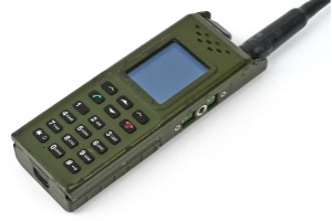
Since its release in 2012, several researchers have discovered that the radio provides built-in protocols to allow communication across multiple standards, including older analogue Russian radios, UAV commands, and even TETRA. While the advertised frequency range is 27 to 520 MHz, recent firmware updates enabled a lower range of frequencies down to 100 kHz with AM.  

The features of this radio are fairly well known. The following was posted by @SomeGumul, a Polish researcher, on Twitter/X:

The trophy in the form of the Russian radio station “Azart”, announced by the Russians as a “native, Russian” sixth-generation device for conducting encrypted conversations, works on American radio components. The basis of the encryption system is, in particular, the Spartan®-6 FPGA (field-programmable gate array) system.  It is produced by the American company XILINX (AMD) in Taiwan.

Ironically, despite being advertised as the forefront of Russia’s military technical prowess, the heart of this device was revealed by Ukrainian serviceman Serhii Flash (Сергей Флэш) to be powered by the Spartan 6 FPGA. This FPGA is what enables the handheld radio’s capabilities to be redefined by mere software updates, allowing its users to speak over virtually any radio standard required—past, present, or future. While most of the currently implemented protocols are unencrypted to allow backward compatibility with other older, active service equipment, communication between two AZART radios enables frequency hopping up to 20,000 frequencies per second. This high rate of frequency hopping creates challenges for eavesdropping and position triangulation. The radio’s implementation of TETRA also supports encryption with the inclusion of a supporting radio trunk, where the radio is referred to as being in Trunked Mode Operation (TMO). Otherwise, while in Direct Mode Operation (DMO), the radio only supports voice scrambling in the time and frequency domains.   

20,000 frequency hops per second is quite a feat for a radio. Extremely precise timing is required for two or more radios to sync across hops and still communicate clearly. This timing source is gained wirelessly from GPS and GLONASS. As such, this advanced feature can be disabled simply by jamming GPS frequencies.

While this attack may be sufficient, GPS signals are ubiquitous and neutral sources of precise timing that are often required by both sides of any conflict. So, while jamming the frequencies may work in a pinch, it would be cleaner to find a solution to track this high rate of frequency hopping without having to jam a useful signal. To find this solution, we must investigate the proprietary Angstrem algorithm that drives the pseudo-random frequency hopping. To do this, we begin by looking at the likely driver: the Spartan 6 FPGA.

Chipset Overview

It is currently unknown if the Spartan 6 on the AZART is utilizing an encrypted bitstream; however, due to its wartime purpose, it must not be ruled out. While waiting for the procurement of a functioning radio, IOActive began a preliminary investigation into the functioning of the Spartan 6 with a specific focus on areas related to encryption and decryption of the bitstream.

Mainboard of AZART Highlighting the Spartan 6

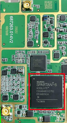
At the time of writing this post, the XC6SLX75-3CSG484I sells for around $227 from authorized US distributors; however, it can be obtained for much lower prices in Asian markets, with sellers on AliExpress listing them for as low as $8.47. While counterfeits are prevalent in these supply chains, legitimate parts are not difficult to obtain with a bit of luck.

In addition to the FPGA, one other notable component visible on the board is the Analog Devices TxDAC AD9747, a dual 16-bit 250 Msps Digital-to-Analog Converter (DAC) intended for SDR transmitters. Assuming this is being used to transmit I/Q waveforms, we can conclude that the theoretical maximum instantaneous bandwidth of the radio is 250 MHz, with the actual bandwidth likely being closer to 200 MHz to minimize aliasing artifacts.

Device Analysis

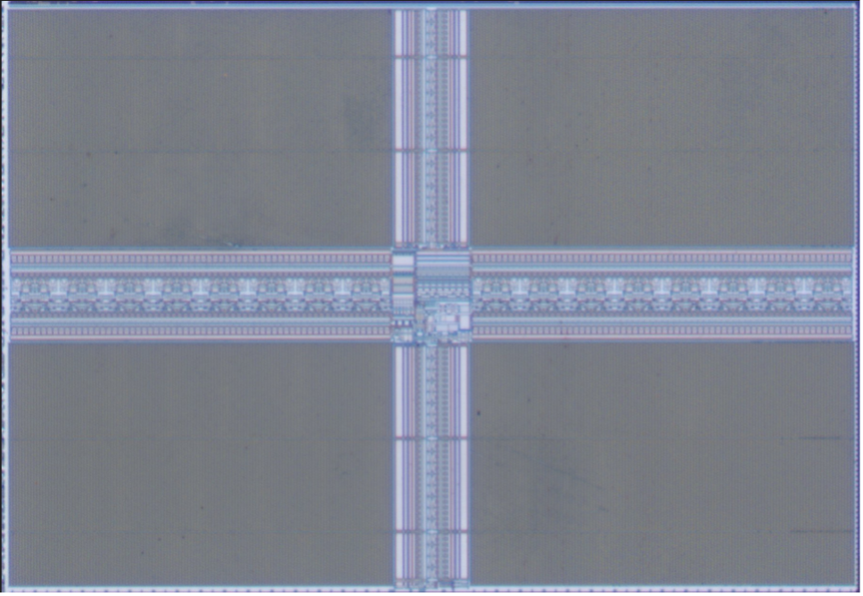
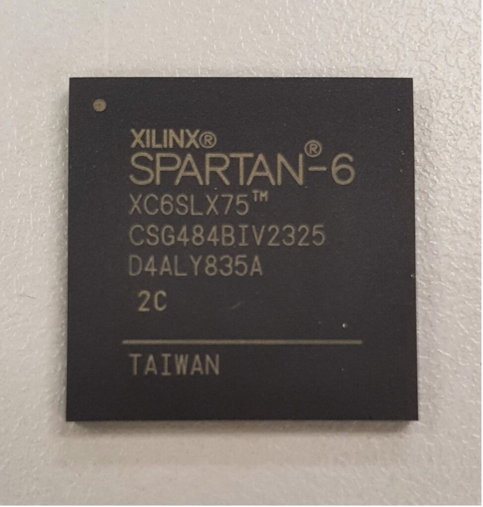
IOActive procured several Spartan 6 FPGAs from a respected supplier for a preliminary silicon teardown to gain insight into how the chip handles encrypted bitstreams and identify any other interesting features. As a standalone package, the Spartan chip looks like this:

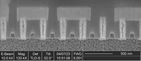
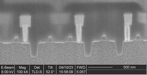
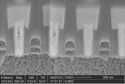
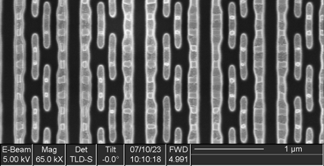
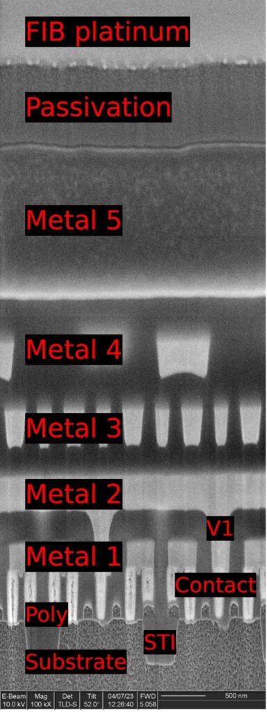
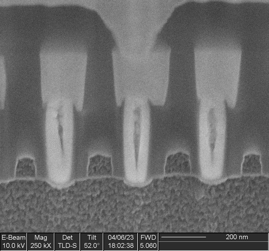
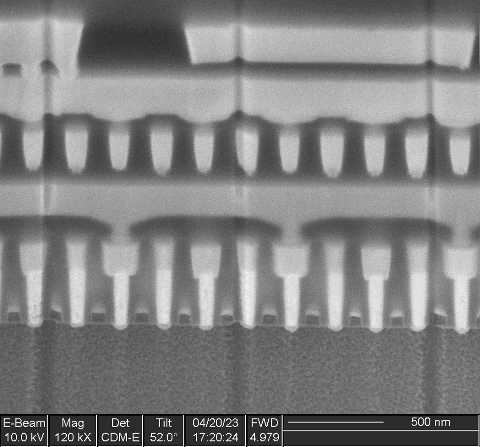
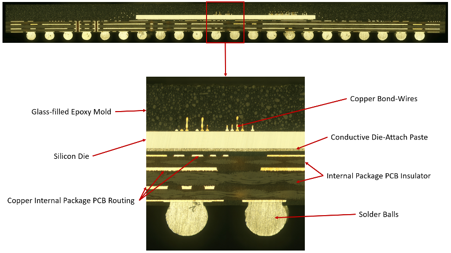
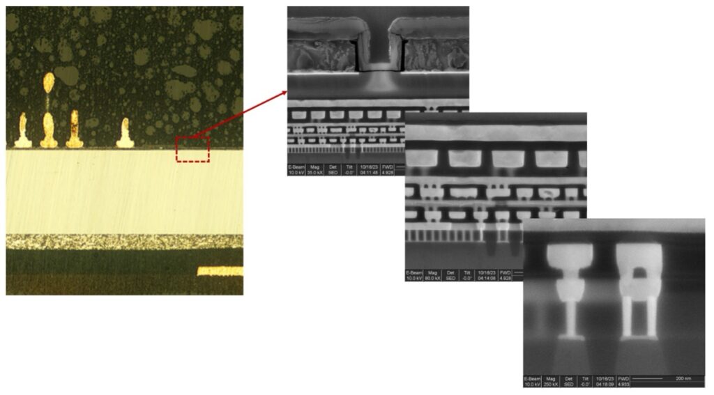
The CSG484 package that contains the Spartan 6 is a wire-bonded Ball-Grid Array (BGA) consisting of the IC die itself (face up), attached by copper ball bonds to a four-layer FR4 PCB substrate and overmolded in an epoxy-glass composite. The substrate has a grid of 22×22 solder balls at 0.8 mm pitch, as can be seen in the following cross section. The solder balls are an RoHS-compliant SAC305 alloy, unlike the “defense-grade” XQ6SLX75, which uses Sn-Pb solder balls. The choice of a consumer-grade FPGA for a military application is interesting, and may have been driven by cost or component availability issues (as the XQ series parts are produced in much lower volume and are not common in overseas supply chains).

Spartan 6 Cross Section Material Analysis

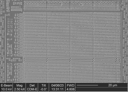
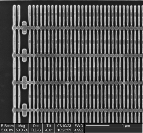
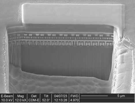
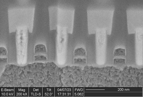
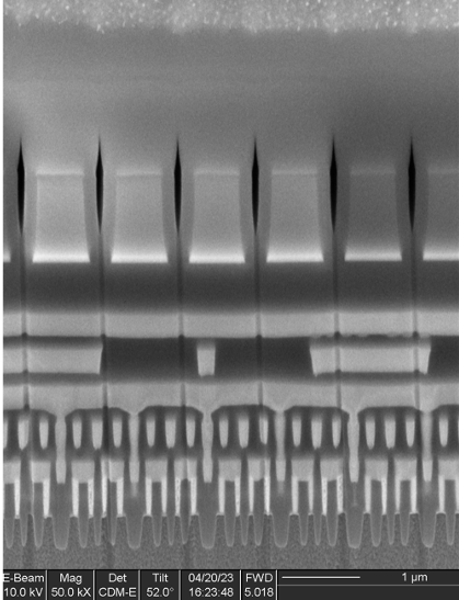
The sample was then imaged in an SEM to gain insight into the metal layers for to order to perform refined deprocessing later. The chip logic exists on the surface of the silicon die, as outlined by the red square in the following figure.

Close-up of FPGA Metal Layers on Silicon Die

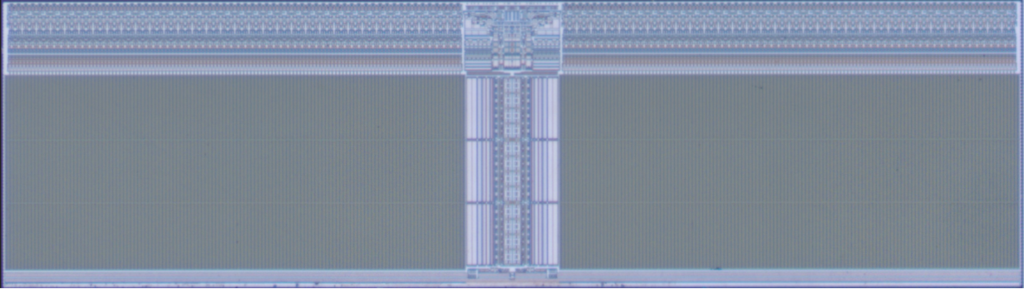
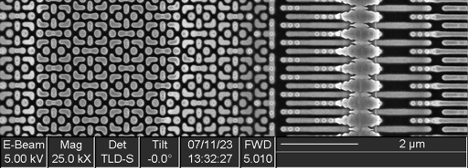
The XC6SLX75 is manufactured by Samsung on a 45 nm process with nine metal layers. A second FPGA was stripped of its packaging for a top-down analysis, starting with metal layer nine.

Optical Overview Image of Decapsulated Die Xilinx XC6SLX75

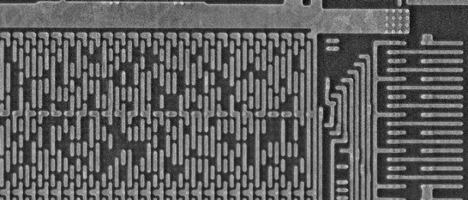
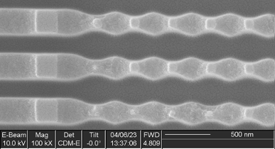
Looking at the top layer, not much structure is visible, as the entire device is covered by a dense grid of power/ground routing. Wire bond pads around the perimeter for power/ground and I/O pins can clearly be seen. Four identical regions, two at the top and two at the bottom, have a very different appearance from the rest of the device. These are pairs of multi-gigabit serial transceivers, GTPs in Xilinx terminology, capable of operation at up to 3.2 Gbps. The transceivers are only bonded out in the XC6SLX75T; the non –T version used in the radio does not connect them, so we can ignore them for the purposes of this analysis.

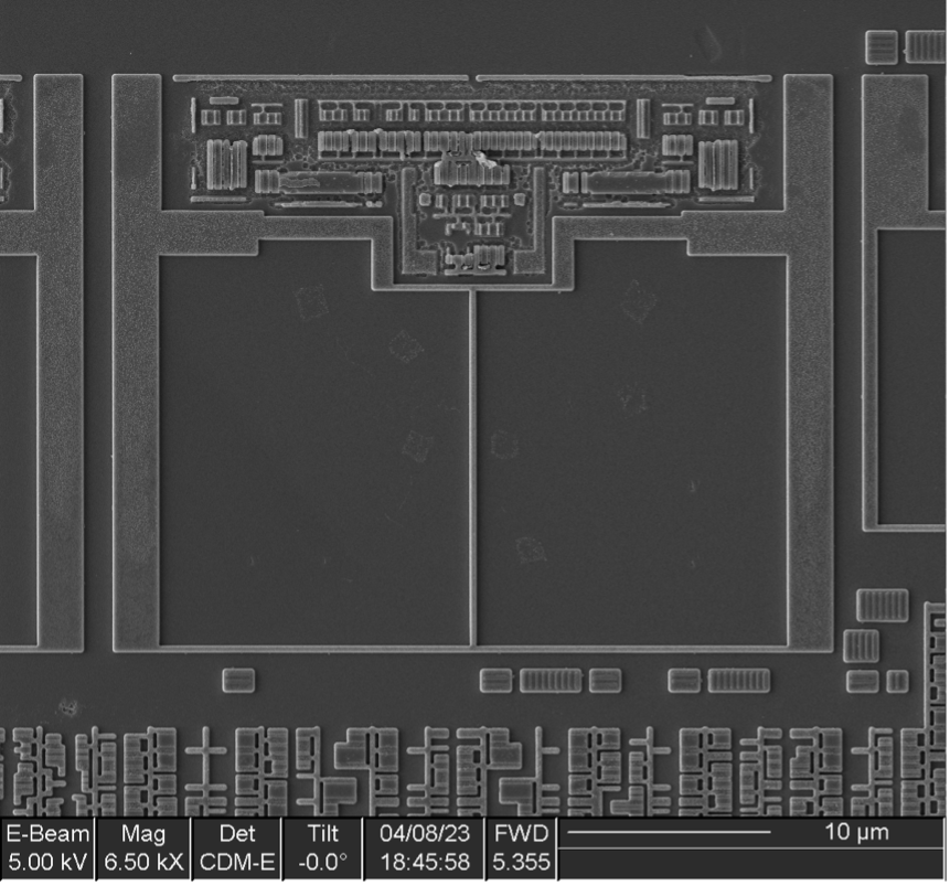
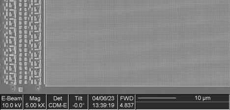
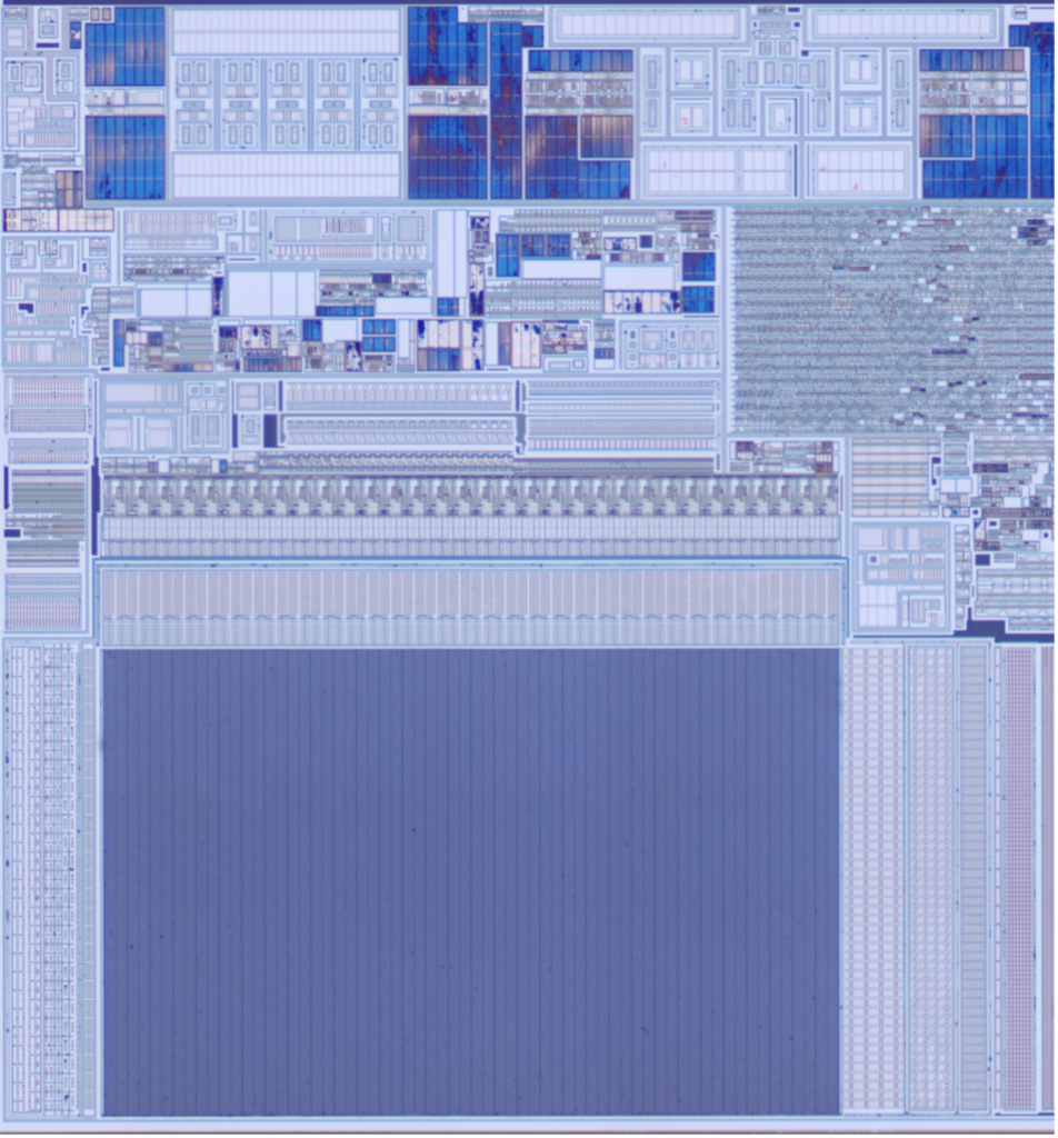
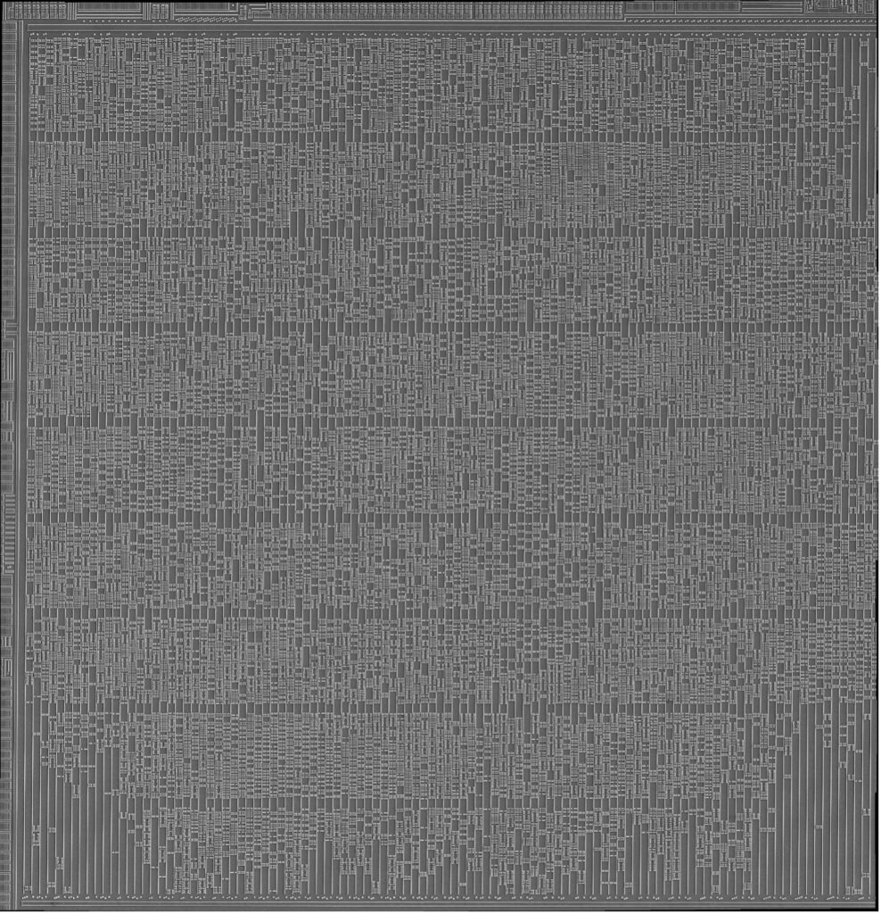
The metal layers were then etched off to expose the silicon substrate layer, which provides better insight into chip layout, as shown in the following figure.

Optical Overview Image of Floorplan of Die Xilinx XC6SLX75

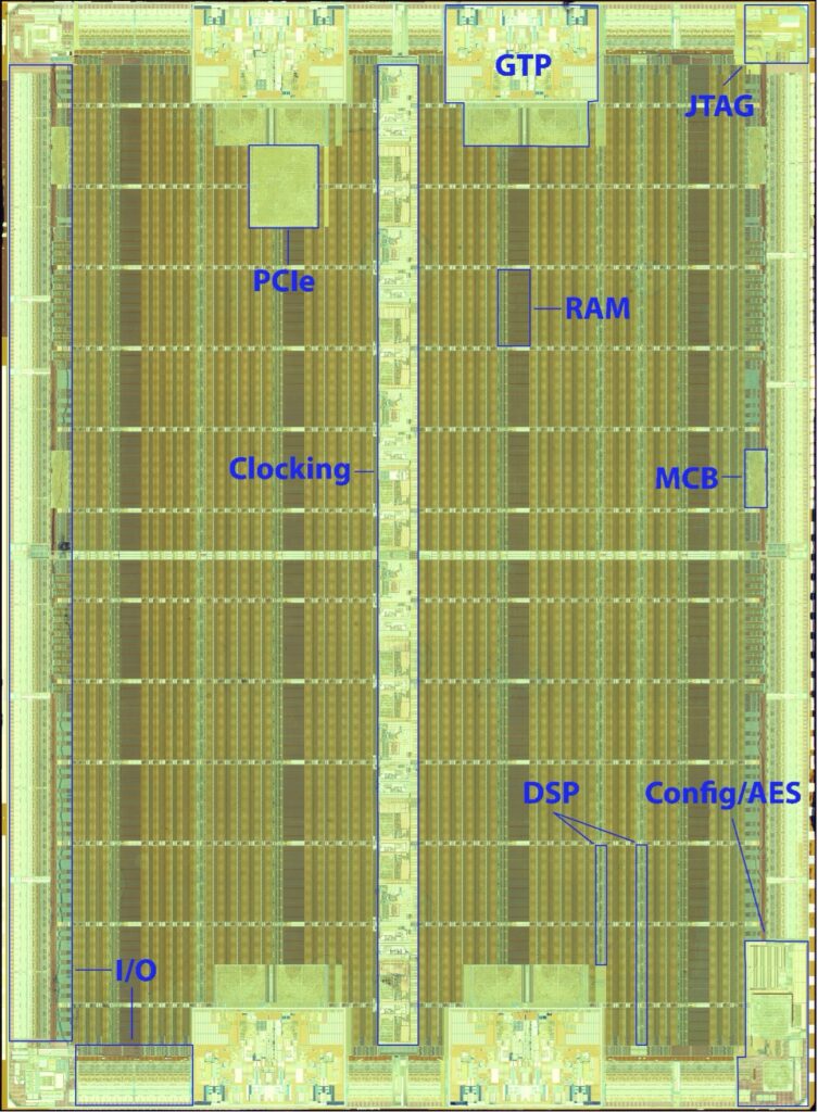
After etching off the metal and dielectric layers, a much clearer view of the device floorplan becomes visible. We can see that the northwest GTP tile has a block of logic just south of it. This is a PCIe gen1 controller, which is not used in the non –T version of the FPGA and can be ignored.

The remainder of the FPGA is roughly structured as columns of identical blocks running north-south, although some columns are shorter due to the presence of the GTPs and PCIe blocks. The non-square logic array of Spartan 6 led to poor performance as user circuitry had to be shoehorned awkwardly around the GTP area. Newer-generation Xilinx parts place the GTPs in a rectangular area along one side of the device, eliminating this issue.

The light-colored column at the center contains clock distribution buffers as well as Phase-Locked Loops (PLLs) and Digital Clock Managers (DCMs) for multiplying or dividing clocks to create different frequencies. Smaller, horizontal clock distribution areas can be seen as light-colored rows throughout the rest of the FPGA.

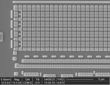
There are four columns of RAM containing a total of 172 tiles of 18 kb, and three columns of DSP blocks containing a total of 132 tiles, each consisting of an 18×18 integer multiplier and some other logic useful for digital signal processing. The remaining columns contain Configurable Logic Blocks (CLBs), which are general purpose logic resources.

The entire perimeter of the device contains I/O pins and related logic. Four light-colored regions of standard cell logic can be seen in the I/O area, two on each side. These are the integrated DDR/DDR2/DDR3 Memory Controller Blocks (MCBs).

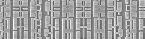
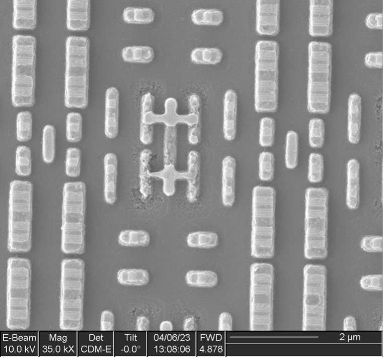
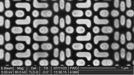
The bottom right contains two larger regions of standard cell logic, which appear related to the boot and configuration process. We expect the eFuse and Battery-Backed SRAM (BBRAM), which likely contain the secrets required to decrypt the bitstream, to be found in this area. As such, this region was scanned in high resolution with the SEM for later analysis.

SEM Substrate Image of Boot/AES Logic Block 1

Utilizing advanced silicon deprocessing and netlist extraction techniques, IOActive hopes to refine methodologies for extracting the configured AES keys required to decrypt the bitstream that drives the Spartan 6 FPGA.

Once this is complete, there is a high probability that the unencrypted bitstream that configures the AZART can be obtained from a live radio and analyzed to potentially enumerate the secret encryption and frequency hopping algorithms that protect the current generation of AZART communications. We suspect that we could also apply this technique to previous generations of AZART, as well as other FPGA-based SDRs like those commonly in use by law enforcement, emergency services, and military operations around the world.

INSIGHTS, RESEARCH | April 17, 2024

Accessory Authentication – part 3/3

This is Part 3 of a 3-Part series. You can find Part 1 here and Part 2 here.

Introduction

In this post, we continue our deep dive comparison of the security processors used on a consumer product and an unlicensed clone. Our focus here will be identifying and characterizing memory arrays.

Given a suitably deprocessed sample, memories can often be recognized as such under low magnification because of their smooth, regular appearance with distinct row/address decode logic on the perimeter, as compared to analog circuitry (which contains many large elements, such as capacitors and inductors) or autorouted digital logic (fine-grained, irregular structure).

Identifying memories and classifying them as to type, allows the analyst to determine which ones may contain data relevant to system security and assess the difficulty and complexity of extracting their content.

OEM Component

Initial low-magnification imaging of the OEM secure element identified 13 structures with a uniform, regular appearance consistent with memory.

Higher magnification imaging resulted in three of these structures being reclassified as non-memory (two as logic and one as analog), leaving 10 actual memories.

Figure 1. Logic circuitry initially labeled as memory due to its regular structure
Figure 2. Large capacitor in analog block

Of the remaining 10 memories, five distinct bit cell structures were identified:

  • Single-port (6T) SRAM
  • Dual-port (8T) SRAM
  • Mask ROM
  • 3T antifuse
  • Floating gate NOR flash

Single-port SRAM

13 instances of this IP were found in various sized arrays, with capacities ranging from 20 bits x 8 rows to 130 bits x 128 rows.

Some of these memories include extra columns, which appear to be intended as spares for remapping bad columns. This is a common practice in the semiconductor industry to improve yield: memories typically cover a significant fraction of the die surface and thus are responsible for a large fraction of manufacturing defects. If the device can remain operable despite a defect in a memory array, the overall yield of usable chips will be higher.

Figure 3. Substrate overview of a single-port SRAM array
Figure 4. Substrate closeup view of single-port SRAM bit cells

Dual-port SRAM

Six instances of this IP were found, each containing 320 bit cells (40 bytes).

Figure 5. Dual-port SRAM cells containing eight transistors

Mask ROM

Two instances of this IP were found, with capacities of 256 Kbits and 320 Kbits respectively. No data was visible in a substrate view of the array.

Figure 6. Substrate view of mask ROM showing no data visible

A cross section (Figure 7) showed irregular metal 1 patterns as well as contacts that did not go to any wires on metal 1, strongly suggesting this was a metal 1 programmed ROM. A plan view of metal 1 (Figure 8) confirms this. The metal 1 pattern also shows that the transistors are connected in series strings of 8 bits (with each transistor in the string either shorted by metal or not, in order to encode a logic 0 or 1 value), completing the classification of this memory as a metal 1 programmed NAND ROM.

Figure 7. Cross section of metal 1 programmed NAND ROM showing irregular metal patterns and via with unconnected top
Figure 8. Top-right corner of one ROM showing data bits and partial address decode logic

IOActive successfully extracted the contents of both ROMs and determined that they were encrypted. Further reverse engineering would be necessary to locate the decryption circuitry in order to make use of the dumps.

Antifuse

Five instances of this IP were found, four with a capacity of 4 rows x 32 bits (128 bits) and one with a capacity of 32 rows x 64 bits (2048 bits).

The bit cells consist of three transistors (two in series and one separate) and likely function by gate dielectric breakdown: during programming, high voltage applied between a MOSFET gate and the channel causes the dielectric to rupture, creating a short circuit between the drain and gate terminals.

Antifuse memory is one-time programmable and is expensive due to the very low density (significantly larger bit cell compared to flash or ROM); however, it offers some additional security because the ruptured dielectric is too thin to see in a top-down view of the array, rendering it difficult to extract the contents of the bit cells. It is also commonly used for small memories when the complexity and re-programmability of flash memory is unnecessary, such as for storing trim values for analog blocks or remapping data for repairing manufacturing defects in SRAM arrays.

Figure 9. Antifuse array
Figure 10. Cross section of antifuse bit cells

Flash

A single instance of this IP was found, with a capacity of 1520 Kbits.

This memory uses floating-gate bit cells connected in a NOR topology, as is common for embedded flash memories on microcontrollers.

Figure 11. Substrate plan view of bit cells
Figure 12. Cross section of NOR Flash memory

Clone Component

Floorplan Overview

Figure 13. Substrate view of clone secure element after removal of metal and polysilicon

The secure element from the clone device contains three obvious memories, located at the top right, bottom left, and bottom right corners.

Lower-left Memory

The lower-left memory consists of a bit cell array with addressing logic at the top, left, and right sides. Looking closely, it appears to be part of a larger rectangular block that contains a large region of analog circuitry above the memory, as well as a small amount of digital logic.

This is consistent with the memory being some sort of flash (likely the primary code and data storage for the processor). The large analog block is probably the high voltage generation for the program/erase circuitry, while the small digital block likely controls timing of program/erase operations.  

The array appears to be structured as 32 bits (plus 2 dummy or ECC columns) x 64 blocks wide, by 2 bits * 202 rows (likely 192 + 2 dummy features + 8 spare). This gives an estimated usable array capacity of 786432 bits (98304 bytes, 96kB).

Figure 14. Overview of bottom left (flash) memory
Figure 15. SEM substrate image of flash memory

A cross section was taken, which did not show floating gates (as compared to the OEM component). This suggests that this component is likely using a SONOS bit cell or similar charge-trapping technology.

Lower-right Memory

The lower-right memory consists of two identical blocks side-by-side, mirrored left-to-right. Each block consists of 128 columns x 64 cells x 3 blocks high, for a total capacity of 49152 bits (6144 bits, 6 kB).

Figure 16. Lower-right memory

At higher magnification, we can see that the individual bit cells consist of eight transistors, indicative of dual-port SRAM—perhaps some sort of cache or register file.

Figure 17. Dual-port SRAM on clone secure element (substrate)
Figure 18. Dual-port SRAM on clone secure element (metal 1)

Upper-right Memory

The upper – right memory consists of a 2 x 2 grid of identical tiles, each 128 columns x 160 rows (total capacity 81920 bits/10240 bytes/10 kB).

Figure 19. Upper-right SRAM array

Upon closer inspection, the bit cell consists of six transistors arranged in a classic single-port SRAM structure.

Figure 20. SEM substrate image of 6T SRAM cells
Figure 21. SEM metal 1 image of 6T SRAM cells

Concluding Remarks

The OEM component contains two more memory types (mask ROM and antifuse) than the clone component. It has double the flash memory and nearly triple the persistent storage (combined mask ROM and flash) capacity of the clone, but slightly less SRAM.

Overall, the memory technology of the clone component is significantly simpler and lower cost.

Overall Conclusions

OEMs secure their accessory markets for the following reasons:

  • To ensure an optimal user experience for their customers
  • To maintain the integrity of their platform
  • To secure their customers’ personal data
  • To secure revenue from accessory sales

OEMs routinely use security chips to protect their platforms and accessories; cost is an issue for OEMs when securing their platforms, which potentially can lead to their security being compromised.

Third-party solution providers, on the other hand:

  • Invest in their own labs and expertise to extract the IP necessary to make compatible solutions
  • Employ varied attack vectors with barriers of entry ranging from non-invasive toolsets at a cost of $1,000 up, to an invasive, transistor-level Silicon Lab at a cost of several million dollars
  • Often also incorporate a security chip to secure their own solutions, and to in turn lock out their competitors
  • Aim to hack the platform and have the third-party accessory market to themselves for as long as possible
INSIGHTS, RESEARCH |

Accessory Authentication – part 2/3

This is Part 2 of a 3-Part series. You can find Part 1 here and Part 3 here.

Introduction

In this post, we continue our deep dive comparison of the security processors used on a consumer product and an unlicensed clone. Our focus here will be comparing manufacturing process technology.

We already know the sizes of both dies, so given the gate density (which can be roughly estimated from the technology node or measured directly by locating and measuring a 2-input NAND gate) it’s possible to get a rough estimate for gate count. This, as well as the number of metal layers, can be used as metrics for overall device complexity and thus difficulty of reverse engineering.

For a more accurate view of device complexity, we can perform some preliminary floorplan analysis of each device and estimate the portions of die area occupied by:

  • Analog logic (generally uninteresting)
  • Digital logic (useful for gate count estimates)
  • RAM (generally uninteresting aside from estimating total bit capacity)
  • ROM/flash (allows estimating capacity and, potentially, difficulty of extraction)

OEM Component

We’ll start with the OEM secure element and take a few cross sections using our dual-beam scanning electron microscope/focused ion beam (SEM/FIB). This instrument provides imaging, material removal, and material deposition capabilities at the nanoscale.

Figure 1. SEM image showing FIB cross section of OEM component

To cross section a device, the analyst begins by using deposition gases to create a protective metal cap over the top of the region of interest. This protects the top surface from damage or contamination during the sectioning process. This is then followed by using the ion beam to make a rough cut a short distance away from the region of interest, then a finer cut to the exact location. The sample can then be imaged using the electron beam.

Figure 1 shows a large rectangular hole cut into the specimen, with the platinum cap at top center protecting the surface. Looking at the cut face, many layers of the device are visible. Upon closer inspection (Figure 2), we can see that this device has four copper interconnect layers followed by a fifth layer of aluminum.

Figure 2. Cross section with layers labeled
Figure 3. Cross-section view of OEM component showing individual transistor channels

At higher magnification (Figure 3), we can clearly see individual transistors. The silicon substrate of the device (bottom) has been etched to enhance contrast, giving it a rough appearance. The polysilicon transistor gates, seen end-on, appear as squares sitting on the substrate. The bright white pillars between the gates are tungsten contacts, connecting the source and drain terminals of each transistor to the copper interconnect above.

Figure 4. 6T SRAM bit cells on OEM component

Based on measurements of the gates, we conclude that this device is made on a 90 nm technology:

  • Contacted gate pitch: 282 nm
  • M1 pitch: 277 nm
  • 6T SRAM bit cell (Figure 4): 1470 x 660 nm (0.97 µm2)

We can also use cross sections to distinguish between various types of memory. Figure 5 is a cross section of one of the memory arrays of the OEM device, showing a distinctive double-layered structure instead of the single polysilicon gates seen in Figure 3. This is a “floating gate” nonvolatile memory element; the upper control gate is energized to select the cell while the lower floating gate stores charge, representing a single bit of memory data.

The presence of metal contacts at both sides of each floating gate transistor (rather than at either end of a string of many bits) allows us to complete the classification of this memory as NOR flash, rather than NAND.

Figure 5. Cross section of NOR flash memory on OEM component showing floating gates

The overall device is approximately 2400 x 1425 µm (3.42 mm2), broken down as:

  • 67% (2.29 mm2): memories and analog IP blocks
  • 33% (1.13 mm2): standard cell digital logic

Multiplying the logic area by an average of published cell library density figures for the 90nm node results in an estimated 475K gates of digital logic (assuming 100% density) for the OEM security processor. The actual gate count will be less than this estimate as there are some dummy/filler cells in less dense areas of the device.

Clone Component

Performing a similar analysis on the clone secure element, we see five copper and one aluminum metal layers (Figure 6).

Figure 6. Cross section of clone security processor showing layers
Figure 7. Closeup of SRAM transistors from clone security processor

Interestingly, the clone secure element is made on a more modern process node than the OEM component:

  • Contacted gate pitch: 225 nm
  • Minimum poly pitch: 158 nm
  • SRAM bit cell: 950 x 465 nm (0.45 µm2)

The transistor gates appear to still be polysilicon rather than metal.

Figure 8. NAND2 cell from clone component, substrate view with metal and polysilicon removed

These values are in-between those reported for the 65 nm and 45 nm nodes, suggesting this device is made on a 55 nm technology. The lack of metal gates (which many foundries began using at the 45 nm node) further reinforces this conclusion.

The overall device is approximately 1190 x 1150 µm (1.36 mm2), broken down as:

  • 37% (0.50 mm2): memories
  • 27% (0.36 mm2): analog blocks and bond pads
  • 31% (0.42 mm2): standard cell digital logic
  • 5% (0.07 mm2): filler cells, seal ring, and other non-functional areas

Given the roughly 0.42 mm2 of logic and measured NAND2 cell size of 717 x 1280 nm (0.92 µm2 or 1.08M gates/mm2 at 100% utilization), we estimate a total gate count of no more than 450K—slightly smaller than the OEM secure element. The actual number is likely quite a bit less than this, as a significant percentage (higher than on the OEM part) of the logic area is occupied by dummy/filler cells.

In part 3, we continue our deep dive comparison of the security processors used on a consumer product and an unlicensed clone. There we will focus on identifying and characterizing the memory arrays.