
In the post “Reading CMOS layout,” we discussed understanding CMOS layout in order to reverse-engineer photographs of a circuit to a transistor-level schematic. This was all well and good, but I glossed over an important (and often overlooked) part of the process: using the photos to observe and understand the circuit’s actual geometry.
Optical Microscopy
Let’s start with brightfield optical microscope imagery. (Darkfield microscopy is rarely used for semiconductor work.) Although reading lower metal layers on modern deep-submicron processes does usually require electron microscopy, optical microscopes still have their place in the reverse engineer’s toolbox. They are much easier to set up and run quickly, have a wider field of view at low magnifications, need less sophisticated sample preparation, and provide real-time full-color imagery. An optical microscope can also see through glass insulators, allowing inspection of some underlying structures without needing to deprocess the device.
This can be both a blessing and a curse. If you can see underlying structures in upper-layer images, it can be much easier to align views of different layers. But it can also be much harder to tell what you’re actually looking at! Luckily, another effect comes to the rescue – depth of field.
Depth of field
When using an objective with 40x power or higher, a typical optical microscope has a useful focal plane of less than 1 µm. This means that it is critical to keep the sample stage extremely flat – a slope of only 100 nm per mm (0.005 degrees) can result in one side of a 10x10mm die being in razor-sharp focus while the other side is blurred beyond recognition.
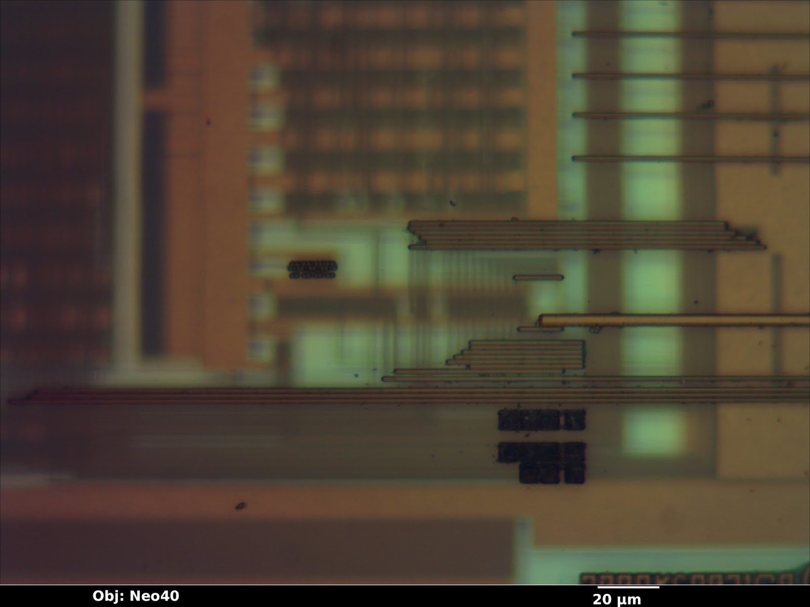
In the image below (from a Micrel KSZ9021RN gigabit Ethernet PHY) the top layer is in sharp focus but all of the features below are blurred—the deeper the layer, the less easy it is to see.
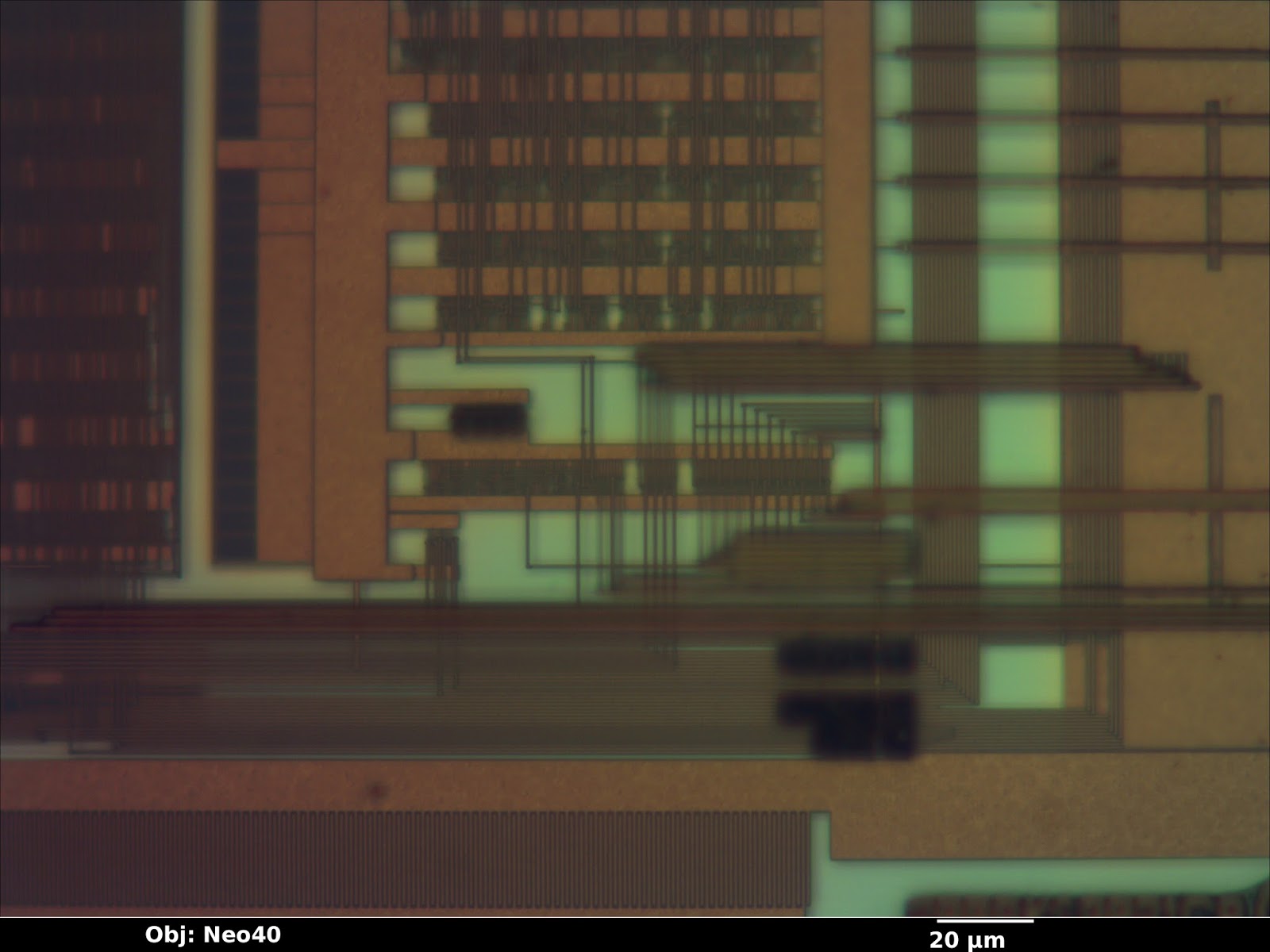
We as reverse engineers can use this to our advantage. By sweeping the focus up or down, we can get a qualitative feel for which wires are above, below, or on the same layer as other wires. Although it can be useful in still photos, the effect is most intuitively understood when looking through the eyepiece and adjusting the focus knob by hand. Compare the previous image to this one, with the focal plane shifted to one of the lower metal layers.
I also find that it’s sometimes beneficial to image a multi-layer IC using a higher magnification than strictly necessary, in order to deliberately limit the depth of field and blur out other wiring layers. This can provide a cleaner, more easily understood image, even if the additional resolution isn’t necessary.
Color
Another important piece of information the optical microscope provides is color. The color of a feature under an optical microscope is typically dependent on three factors:
- Material color
- Orientation of the surface relative to incident light
- Thickness of the glass/transparent material over it
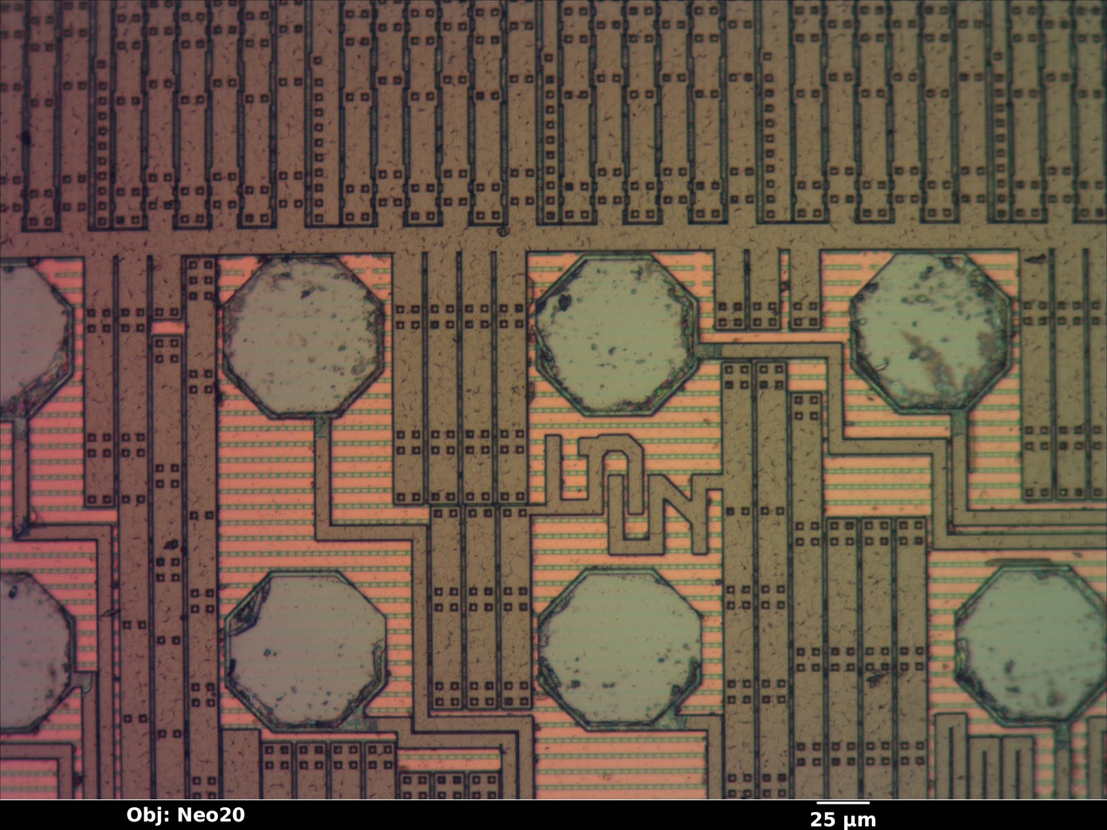
Material color is the easiest to understand. A flat, smooth surface of a substance with nothing on top will have the same color as the bulk material. The octagonal bond pads in the image below (a Xilinx XC3S50A FPGA), for example, are made of bare aluminum and show up as a smooth silvery color, just as one would expect. Unfortunately, most materials used in integrated circuits are either silvery (silicon, polysilicon, aluminum, tungsten) or clear (silicon dioxide or nitride). Copper is the lone exception.
Orientation is another factor to consider. If a feature is tilted relative to the incident light, it will be less brightly lit. The dark squares in the image below are vias in the upper metal layer which go down to the next layer; the “sag” in the top layer is not filled in this process so the resulting slopes show up as darker. This makes topography visible on an otherwise featureless surface.
The third property affecting observed color of a feature is the glass thickness above it. When light hits a reflective surface under a transparent, reflective surface, some of the beam bounces off the lower surface and some bounces off the top of the glass. The two beams interfere with each other, producing constructive and destructive interference at wavelengths equal to multiples of the glass thickness.
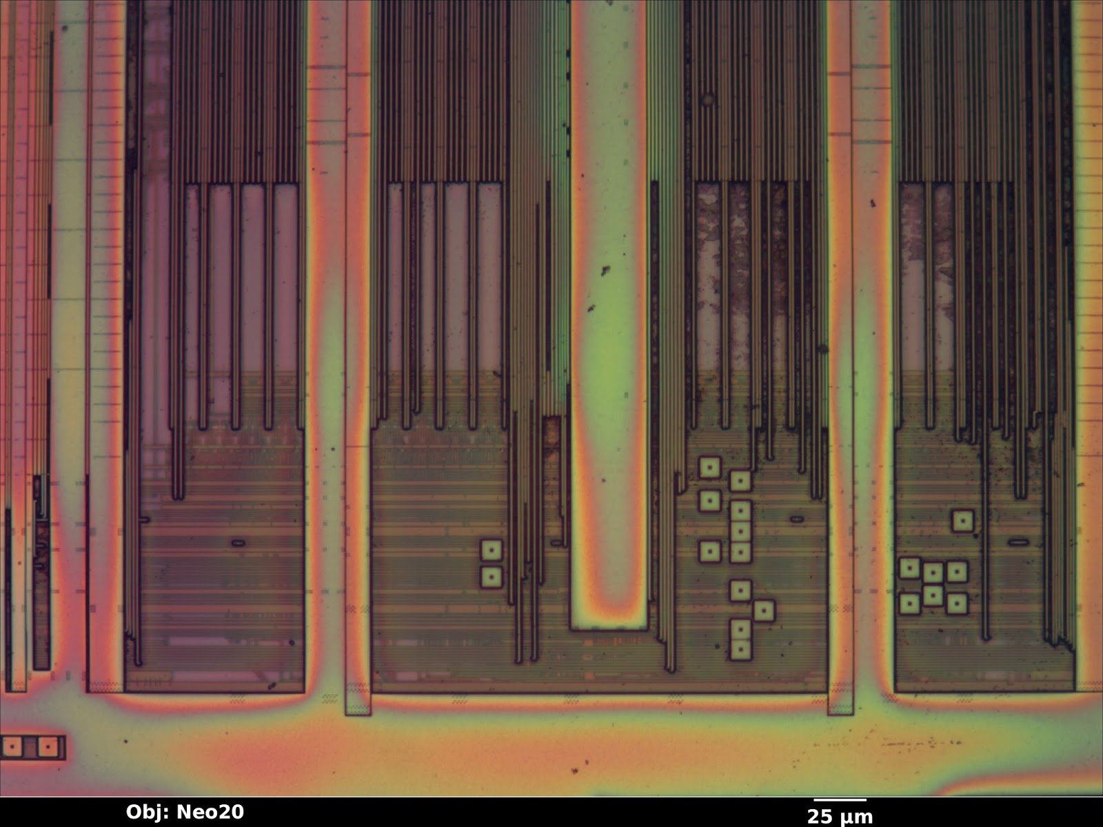
This is the same effect responsible for the colors seen in a film of oil floating on a puddle of water–the reflections from the oil’s surface and the oil-water interface interfere. Since the oil film is not exactly the same thickness across the entire puddle, the observed colors vary slightly. In the image above, the clear silicon nitride passivation is uniform in thickness, so the top layer wiring (aluminum, mostly for power distribution) shows up as a uniform tannish color. The next layer down has more glass over it and shows up as a slightly different pink color.
Compare that to the image below (an Altera EPM3064A CPLD). The thickness of the top passivation layer varies significantly across the die surface, resulting in rainbow-colored fringes.
Electron Microscopy
The scanning electron microscope is the preferred tool for imaging finer pitch features (below about 250 nm). Due to the smaller wavelength of electron beams as compared to visible light, this tool can obtain significantly higher resolutions.
The basic operating principle of a SEM is similar to an old-fashioned CRT display: electromagnets move a beam of electrons in a vacuum chamber in a raster-scan pattern over the sample. At each pixel, the beam interacts with the sample, producing several forms of radiation that the microscope can detect and use for imaging.
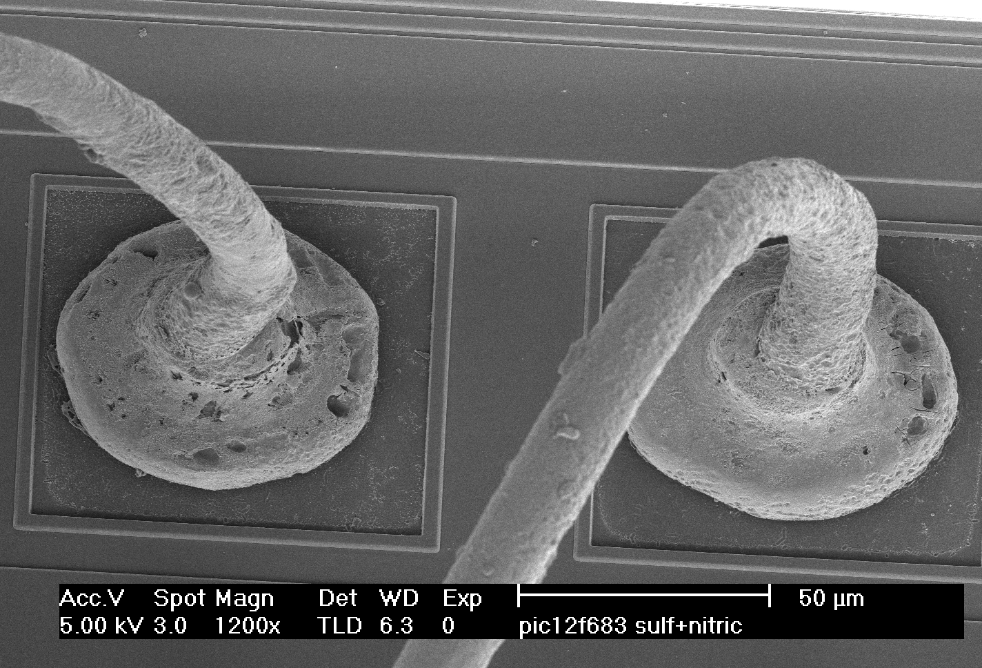
Electron microscopy in general has an extremely high depth of field, making it very useful for imaging 3D structures. The image below (copper bond wires on a Microchip PIC12F683) has about the same field of view as the optical images from the beginning of this article, but even from a tilted perspective the entire loop of wire is in sharp focus.
Secondary Electron Images
The most common general-purpose image detector for the SEM is the secondary electron detector. When a high-energy electron from the scanning beam grazes an atom in the sample, it sometimes dislodges an electron from the outer shell. Secondary electrons have very low energy, and will slow to a stop after traveling a fairly short distance. As a result, only those generated very near the surface of the sample will escape and be detected.
This makes secondary electron images very sensitive to topography. Outside edges, tilted surfaces, and small point features (dust and particulates) show up brighter than a flat surface because a high percentage of the secondary electrons are generated near exposed surfaces of the specimen. Inward-facing edges show up dimmer than a flat surface because a high percentage of the secondary electrons are absorbed in the material.
The general appearance of a secondary electron image is similar to a surface lit up with a floodlight. The eye position is that of the objective lens, and the “light source” appears to come from the position of the secondary electron detector.
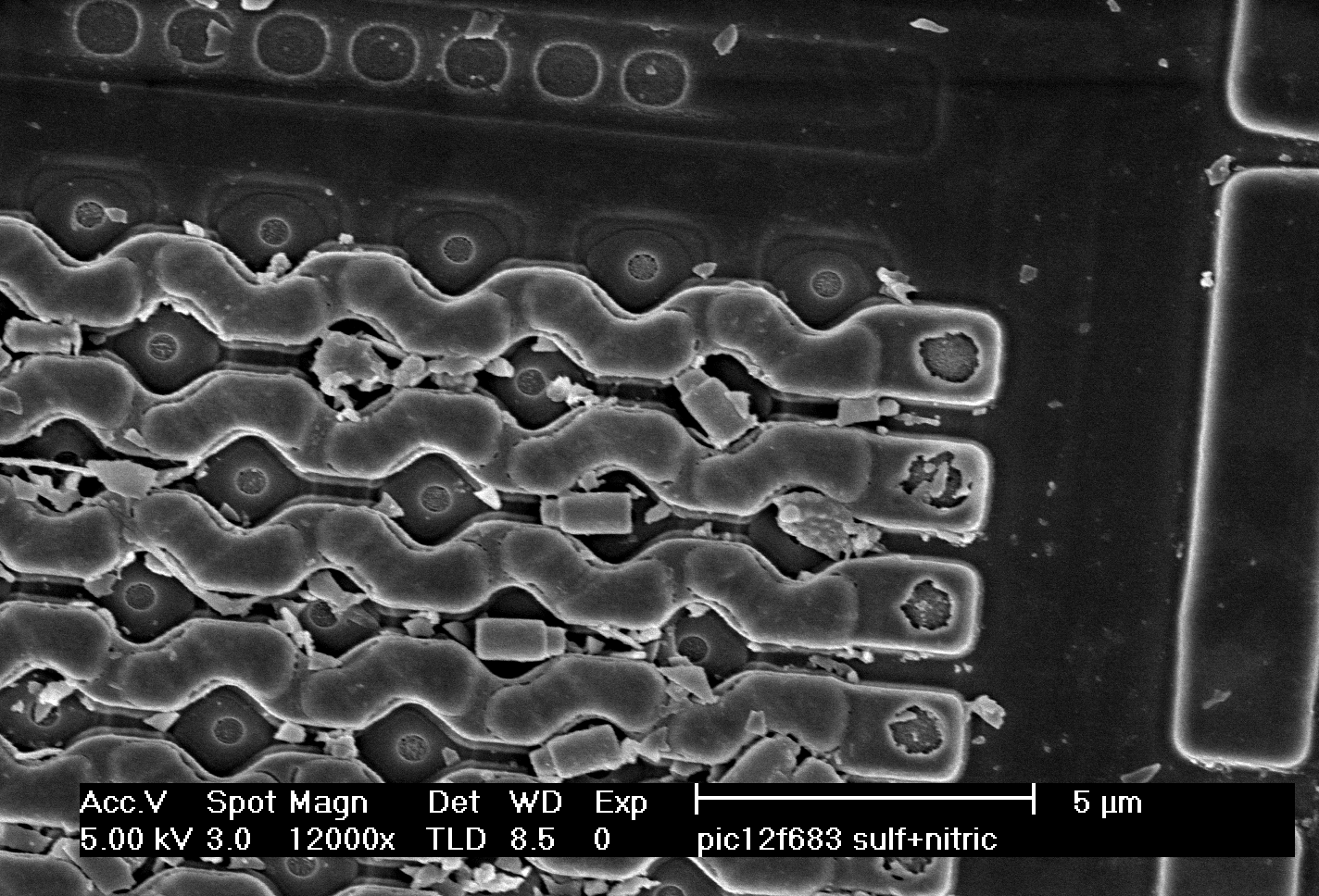
In the image below (the polysilicon layer of a Microchip PIC12F683 before cleaning), the polysilicon word lines running horizontally across the memory array have bright edges, which shows that they are raised above the background. The diamond-shaped source/drain areas have dark “shadowed” edges, showing that they are lower than their surroundings (and thus many of the secondary electrons are being absorbed). The dust particles and loose tungsten via plugs scattered around the image show up very brightly because they have so much exposed surface area.
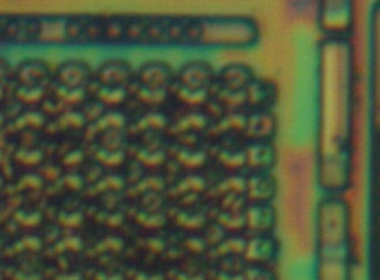
Compare the above SEM view to the optical image of the same area below. Note that the SEM image has much higher resolution, but the optical image reveals (through color changes) thickness variations in the glass layer that are not obvious in the SEM. This can be very helpful when trying to gauge progress or uniformity of an etch/polish operation.
In addition to the primary contrast mechanism discussed above, the efficiency of secondary electron emission is weakly dependent on the elemental composition of the material being observed. For example, at 20 kV the number of secondary electrons produced for a given beam current is about four times higher for tungsten than for silicon (see this paper). While this may lead to some visible contrast in a secondary electron image, if elemental information is desired, it would be preferable to use a less topography-sensitive imaging mode.
Backscattered Electron Images
Secondary electron imaging does not work well on flat specimens, such as a die that has been polished to remove upper metal layers or a cross section. Although it’s often possible to etch such a sample to produce topography for imaging in secondary electron mode, it’s usually easier to image the flat sample using backscatter mode.
When a high-energy beam electron directly impacts the nucleus of an atom in the sample, it will bounce back at high speed in the approximate direction it came from. The probability of such a “backscatter” event happening depends on the atomic number Z of the material being imaged. Since backscatters are very energetic, the surrounding material does not easily absorb them. As a result, the appearance of the resulting image is not significantly influenced by topography and contrast is primarily dependent on material (Z-contrast).
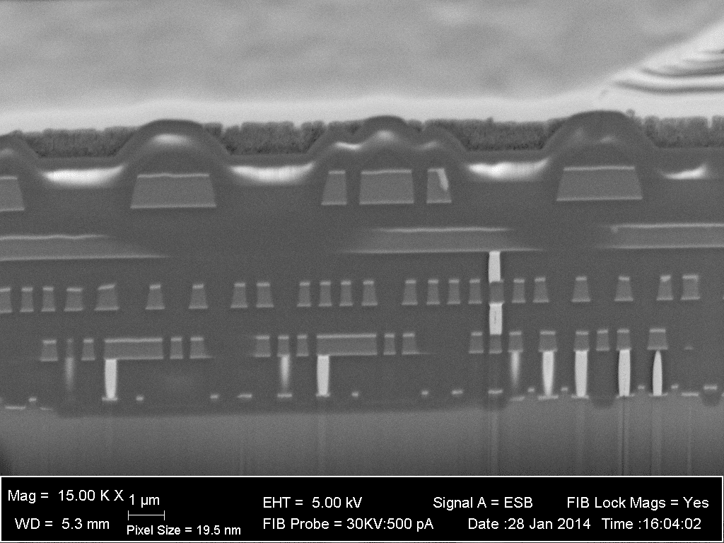
In the image below (cross section of a Xilinx XC2C32A CPLD), the silicon substrate (bottom, Z=14) shows up as a medium gray. The silicon dioxide insulator between the wires is darker due to the lower average atomic number (Z=8 for oxygen). The aluminum wires (Z=13) are about the same color as the silicon, but the titanium barrier layer (Z=22) above and below is significantly brighter. The tungsten vias (Z=74) are extremely bright white. Looking at the bottom right where the via plugs touch the silicon, a thin layer of cobalt (Z=27) silicide is visible.
Depending on the device you are analyzing, any or all of these three imaging techniques may be useful. Knowledge of the pros and cons of these techniques and the ability to interpret their results are key skills for the semiconductor reverse engineer.