
In Spain we have a saying “Hecha la ley, hecha la trampa” which basically means there will always be a way to circumvent a restriction. In fact, that is pretty much what hacking is all about.
It seems the idea of ‘counterfeiting’ appeared at the same time as legitimate money. The Wikipedia page for Counterfeit money is a fascinating read that helps explain its effects.
http://en.wikipedia.org/wiki/Counterfeit_money
Nowadays every physical currency implements security measures to prevent counterfeiting. Some counterfeits can be detected with a naked eye, while others need specific devices or procedures to be identified. In order to help employees, counterfeit money detectors can be found in places that accept cash, including shops, malls, postal offices, banks, and gas stations.
 Recently I took a look at one of these devices, Secureuro. I chose this device because it is widely used in Spain, and its firmware is freely available to download.
http://www.securytec.es/Informacion/clientes-de-secureuro
As usual, the first thing I did when approaching a static analysis of a device of this kind was to collect as much information as possible. We should look for anything that could help us to understand how the target works at all levels.
In this case I used the following sources:
Youtube
http://www.youtube.com/user/EuroSecurytec
I found some videos where the vendor details how to use the device. This let me analyze the behavior of the device, such as when an LED turns on, when a sound plays, and what messages are displayed. This knowledge is very helpful for understanding the underlying logic when analyzing the assembler later on.
Vendor Material
Technical specs, manuals, software, firmware … [1] [2] [3] See references.
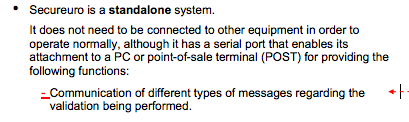
The following document provides some insights into the device’s security http://www.secureuro.com/secureuro/ingles/MANUALINGLES2006.pdf (resource no longer available)
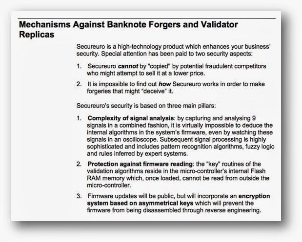
Unfortunately, some of these claims are not completely true and others are simply false. It is possible to understand how Secureuro works; we can access the firmware and EEPROM without even needing hardware hacking. Also, there is no encryption system protecting the firmware.
Before we start discussing the technical details, I would like to clarify that we are not disclosing any trick that could help criminals to bypass the device ‘as is’. My intention is not to forge a banknote that could pass as legitimate, that is a criminal offense. My sole purpose is to explain how I identified the code behind the validation in order to create ‘trojanized’ firmware that accepts even a simple piece of paper as a valid currency. We are not exploiting a vulnerability in the device, just a design feature.
Analyzing the Firmware
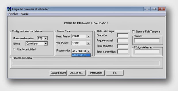
This is the software that downloads the firmware into the device. The firmware file I downloaded from the vendor’s website contains 128K of data that will be flashed to the ATMEGA128 microcontroller. So I can directly load it into IDA, although I do not have access to the EEPROM yet.
Entry Points
A basic approach to dealing with this kind of firmware is to identify some elements or entry points that can leveraged to look for interesting pieces of code.
A minimal set includes:
Interruption Vector
- RESET == Main Entry Point
- TIMERs
- UARTs
- SPI
Mnemonics
- LPM (Load Program Memory)
- SPM (Store Program Memory)
- IN
- OUT
Registers
ADCL: The ADC Data Register Low
ADCH: The ADC Data Register High
ADCSRA: ADC Control and Status Register
ADMUX: ADC Multiplexer Selection Register
ACSR: Analog Comparator Control and Status
UBRR0L: USART Baud Rate Register
UCSR0B: USART Control and Status Register
UCSR0A: USART Control and Status Register
UDR0: USART I/O Data Register
SPCR: SPI Control Register
SPSR: SPI Status Register
SPDR: SPI Data Register
EECR: EEPROM Control Register
EEDR: EEPROM Data Register
EEARL: EEPROM Address Register Low
EEARH: EEPROM Address Register High
OCR2: Output Compare Register
TCNT2: Timer/Counter Register
TCCR2: Timer/Counter Control Register
OCR1BL: Output Compare Register B Low
OCR1BH: Output Compare Register B High
OCR1AL: Output Compare Register A Low
OCR1AH: Output Compare Register A High
TCNT1L: Counter Register Low Byte
TCNT1H: Counter Register High Byte
TCCR1B: Timer/Counter1 Control Register B
TCCR1A: Timer/Counter1 Control Register A
OCR0: Timer/Counter0 Output Compare Register
TCNT0: Timer/Counter0
TCCR0: Timer/Counter Control Register
TIFR: Timer/Counter Interrupt Flag Register
TIMSK: Timer/Counter Interrupt Mask Register
Using this information, we should reconstruct some firmware functions to make it more reverse engineering friendly.
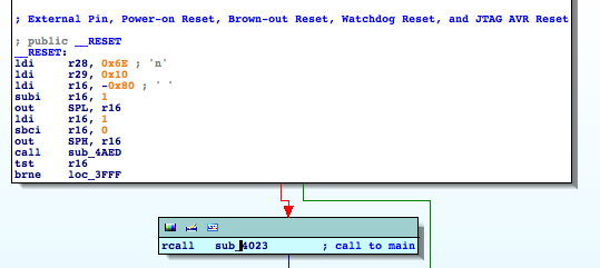
First, I try to identify the Main, following the flow at the RESET ISR. This step is pretty straightforward.
As an example of collecting information based on the mnemonics, we identify a function reading from flash memory, which is renamed to ‘readFromFlash‘. Its cross-references will provide valuable information.
By finding the references to the registers involved in EEPROM operations I come across the following functions ‘sub_CFC‘ and ‘sub_CF3‘:
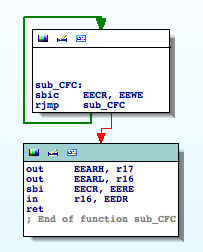
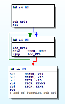
The first routine reads from an arbitrary address in the EEPROM. The second routine writes to the EEPROM. I rename ‘sub_CFC‘ to ‘EEPROM_read‘ and ‘sub_CF3‘ to ‘EEPROM_write‘. These two functions are very useful, and provide us with important clues.
Now that our firmware looks like a little bit more friendly, we focus on the implemented functionalities. The documentation I collected states that this device has been designed to allow communications with a computer; therefore we should start by taking a look at the UART ISRs.
Tip: You can look for USART configuration registers UCSR0B, UBRR0… to see how it is configured.
USART0_RX
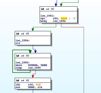
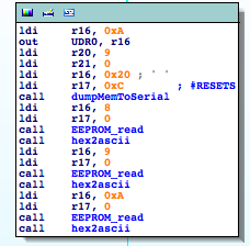
It is definitely interesting, when receiving a ‘J’ (0x49) character it initializes the usual procedure to send data through the serial interface. It checks UDRE until it is ready and then sends outs bytes through UDR0. Going down a little bit I find the following piece of code
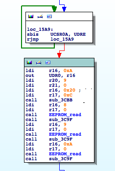
It is using the function to read from the EEPROM I identified earlier. It seems that if we want to understand what is going on we will have to analyze the other functions involved in this basic block, ‘sub_3CBB‘ and ‘sub_3C9F‘.
SUB_3CBB
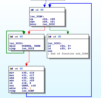
This function is receiving two parameters, a length (r21:r20) and a memory address (r17:r16), and transmitting the n bytes located at the memory address through UDR0. It basically sends n bytes through the serial interface.
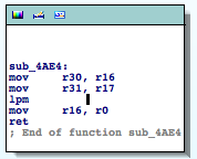
I rename ‘sub_3CBB’ to ‘dumpMemToSerial‘. So this function being called in the following way: dumpMemToSerial(0xc20,9). What’s at address 0xc20? Apparently nothing that makes sense to dump out. I must be missing something here. What can we do? Let’s analyze the stub code the linker puts at the RESET ISR, just before the ‘Main’ entry point. That code usually contains routines for custom memory initialization.
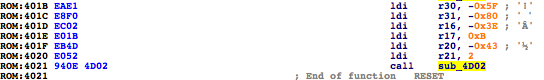
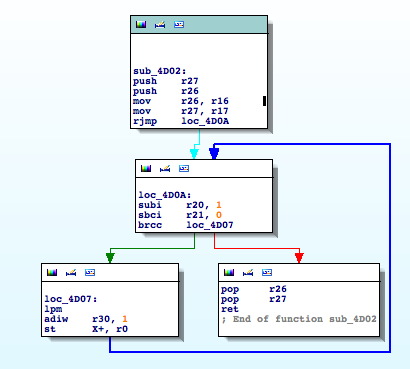
Good enough, ‘sub_4D02‘ is a memory copy function from flash to SRAM. It uses LPM so it demonstrates how important it is to check specific mnemonics to discover juicy functions.
Now take a look at the parameters, at ROM:4041 it is copying 0x2BD bytes (r21:r20) from 0x80A1 (r31:r30) to 0xBC2 (r17:r16). If we go to 0x80A1 in the firmware file, we will find a string table!
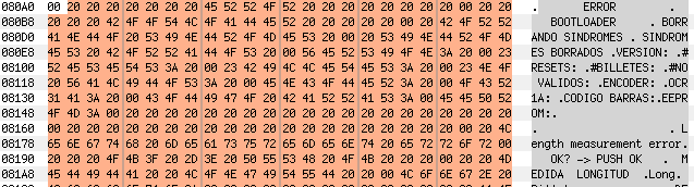
Knowing that 0xBC2 has the string table above, my previous call makes much more sense now: dumpMemToSerial(0xc20,9) => 0xC20 – 0xBC2 = 0x5E
String Table (0x80A1) + 0x5E == “#RESETS”
The remaining function to analyze is ‘sub_3C9F‘, which is basically formatting a byte to its ASCII representation to send it out through the serial interface. I rename it ‘hex2ascii‘
So, according to the code, if we send ‘J’ to the device, we should be receiving some statistics. This matches what I read in the documentation.
http://www.secureuro.com/secureuro/ingles/MANUALINGLES2006.pdf
Now this basic block seems much clearer. It is ‘printing’ some internal statistics.
“#RESETS: 000000” where 000000 is a three byte counter
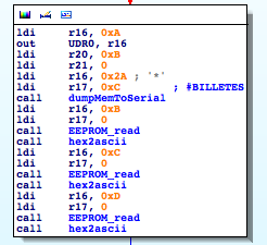
(“BILLETES” means “BANKNOTES” in Spanish)
“#BILLETES: 000000 “
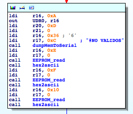
(“NO VALIDOS” means “INVALIDS” in Spanish)
#NO VALIDOS: 000000
…
Wait, hold on a second, the number of invalid banknotes is being stored in a three byte counter in the EEPROM, starting at position 0xE. Are you thinking what I’m thinking? We should look for the opposite operation. Where is that counter being incremented? That path would hopefully lead us to the part of code where a banknote is considered valid or invalid 🙂 Keep calm and ‘EEPROM_write’
Bingo!
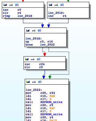
Function ‘sub_1FEB’ (I rename it ‘incrementInvalid’) is incrementing the INVALID counter. Now I look for where it is being called.
‘incrementInvalid‘ is part of a branch, guess what’s in the other part?
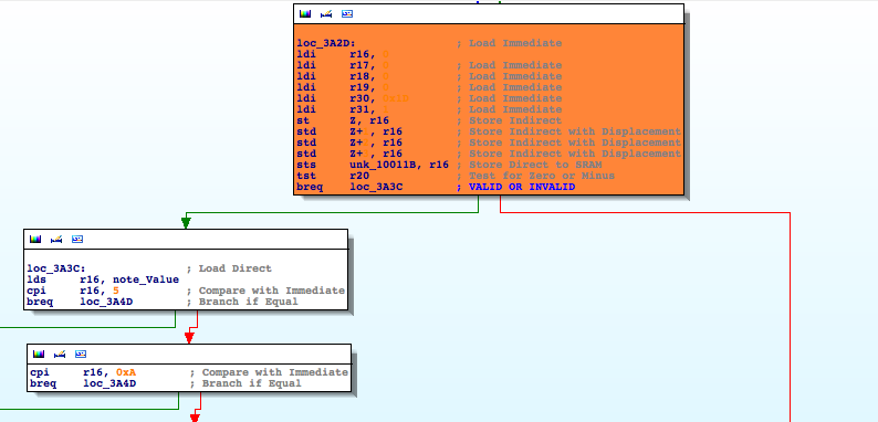
In the left side of the branch, a variable I renamed ‘note_Value’, is being compared against 5 (5€) 0xA (10€). On the other hand, the right side of the branch leads to ‘incrementInvalid‘. Mission accomplished! We found the piece of code where the final validation is performed.
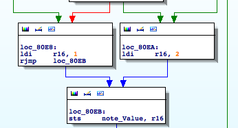
Without entering into details, but digging a little bit further by checking where ‘note_Value’ is being referenced, I easily narrow down the scope of the validation to two complex functions. The first one assigns a value of either 1 or 2 to ‘note_Value’ :
The second function takes into account this value to assigns the final value. When ‘note_Value’ is equal to 1, the possible values for the banknotes are: 5,10, and 20. Otherwise the values should be 50, 100, 200, or 500. Why?
I need to learn about Euro banknotes, so I take a look at the “Trainer’s guide to the Eurobanknotes and coins” from the European Central Bank http://www.ecb.europa.eu/euro/pdf/material/Trainer_A4_EN_SPECIMEN.pdf
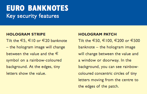
Curious, this classification makes what I see in the code actually make sense. Maybe, only maybe, the first function is detecting the hologram type, and the second function is processing the remaining security features and finally assigning the value. The documentation from the vendor states:
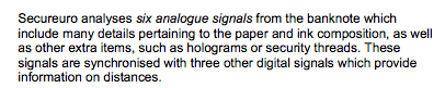
Well, what about those six analogue signals? By checking for the registers involved in ADC operations we are able to identify an interesting function that I rename ‘getAnalogToDigital‘
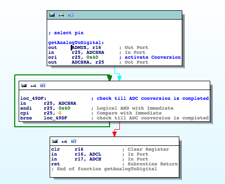
This function receives the input pin from the ADC conversion as a parameter. As expected, it is invoked to complete the conversion of six different pins; inside a timer. The remaining three digital signals with information about the distances can also be obtained easily.
There are a lot of routines we could continue reconstructing: password, menu, configurations, timers, hidden/debug functionalities, but that is outside of the scope of this post. I merely wanted to identify a very specific functionality.
The last step was to buy the physical device. I modified the original firmware to accept our home-made IOActive currency, and…what do you think happened? Did it work? Watch the video to find it out 😉
The impact is obvious. An attacker with temporary physical access to the device could install customized firmware and cause the device to accept counterfeit money. Taking into account the types of places where these devices are usually deployed (shops, mall, offices, etc.) this scenario is more than feasible.
Once again we see that when it comes to static analysis, collecting information about the target is as important as reverse engineering its code. Without the knowledge gained by reading all of those documents and watching the videos, reverse engineering would have been way more difficult.
I hope you find this useful in some way. I would be pleased if this post encourages you to research further or helps vendors understand the importance of building security measures into these types of devices.
References:
[1]http://www.inves.es/secureuro?p_p_id=56_INSTANCE_6CsS&p_p_lifecycle=0&p_p_state=normal&p_p_mode=view&p_p_col_id=detalleserie&p_p_col_count=1&_56_INSTANCE_6CsS_groupId=18412&_56_INSTANCE_6CsS_articleId=254592&_56_INSTANCE_6CsS_tabSelected=3&templateId=TPL_Detalle_Producto
[2] http://www.secureuro.com/secureuro/ingles/menuingles.htm#
[3] http://www.secureuro.com/secureuro/ingles/MANUALINGLES2006.pdf
[4] http://www.youtube.com/user/EuroSecurytec