Antifuse-based OTP Memory Attack May Compromise Cryptographic Secrets
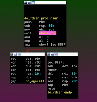
Complementary metal-oxide semiconductor (CMOS) one-time programmable (OTP) memories based on antifuses are widely used for storing small amounts of data (such as serial numbers, keys, and factory trimming) in integrated circuits (ICs) because they are inexpensive and require no additional mask steps to fabricate. The RP2350 uses an off-the-shelf Synopsys antifuse memory block for storing secure boot keys and other sensitive configuration data.
Despite antifuses being widely considered a ”high security” memory—which means they are significantly more difficult for an attacker to extract data from than other types of memory, such as flash or mask ROM—IOActive has demonstrated that data bits stored in the example antifuse memory can be extracted using a well-known semiconductor failure analysis technique: passive voltage contrast (PVC) with a focused ion beam (FIB).
The simple form of the attack demonstrated here recovers the bitwise OR of two physically adjacent memory bitcell rows sharing common metal 1 contacts, however, we believe it is possible for an attacker to separate the even/odd row values with additional effort.
Furthermore, it is highly likely that all products using the Synopsys dwc_nvm_ts40* family of memory IPs on the TSMC 40nm node are vulnerable to the same attack, since the attack is not specific to the RP2350 but rather against the memory itself.
IOActive has not yet tested our technique against other vendors’ antifuse intellectual property (IP) blocks or on other process nodes. Nonetheless, IOActive assessed it to have broad applicability to antifuse-based memories.
Security models which mandate a per-device cryptographic secret are not exposed to significant additional risk, but products which have a shared cryptographic secret stored in the antifuse-based OTP memory are at substantial additional risk from the compromise of a shared secret through this invasive attack.
BACKGROUND
IOActive’s Advanced Low-level Hardware Attacks
IOActive has been building out the depth and coverage of our full-stack cybersecurity assessment capabilities for decades. In recent years, we have been developing exciting new capabilities to dive deeper into the lowest levels of the technology stack using non-invasive, semi-invasive, and fully invasive hardware attack techniques. The key areas of recent focus have been on side channel analysis, fault injection, and fully invasive microchip and IC attacks.
We’ve published original research on side channel analysis on electromechanical locks and fault injection attacks on uncrewed aerial systems (UAS) to demonstrate our capabilities and bring attention to these impactful attack vectors. We’ve been looking for some research projects to demonstrate our fully invasive attack techniques and an industry leader gave us a great opportunity.
IOActive will be sharing more materials in the coming months about advanced, low-level hardware attacks.
Raspberry Pi
Raspberry Pi has an excellent record of producing innovative low-cost, high-value computing hardware that is a favorite of hobbyists, hackers, product designers, and engineers. IOActive has used numerous Raspberry Pi products in our research projects and specialized internal tools to support our commercial cybersecurity engagements. One of the more recent IOActive uses of Raspberry Pi hardware was to build an upgraded remote testing device (RTD) that allowed us to continue delivering our cybersecurity assessments during the pandemic that previously required our consultants to be on site at a client’s facility. The RTD allowed us to continue operating during the lockdowns and Raspberry Pi allowed us to do so with a high-performance, low-cost device. It’s fair to say we’re fans.
RP2350
The RP2350 microcontroller is a unique dual-core, dual-architecture with a pair of industry-standard Arm Cortex-M33 cores and a pair of open-hardware Hazard3 RISC-V cores. It was used as a key component in the DEF CON 2024 (DEF CON 32) Human badge. IOActive sponsored the 2024 car hacking badge for DEF CON’s Car Hacking Village. IOActive has participated in DEF CON since our founding. Companies who participate in DEF CON demonstrate an above average commitment to cybersecurity and the security of their products.
The RP2350 datasheet and product brief highlight the significant effort that Raspberry Pi made into democratizing the availability of modern security features in the RP2350. The RP2350 provides support for Arm TrustZone for Cortex-M, signed boot, 8-KB of antifuse OTP memory for cryptographic key storage, SHA-256 acceleration, a hardware true random number generator (TRNG), and fast glitch detectors.
IOActive strongly recommends that users of the RP2350 employ these advanced security features.
RP2350 Security Challenge
Building on their commitment to product security, the Raspberry Pi team, in addition to participating in DEF CON, also sponsored a Hacking Challenge using the RP2350 with a bug bounty. The objective or “flag” of this challenge was to “find an attack that lets you dump a secret hidden in OTP ROW 0xc08 – the secret is 128-bit long and protected by OTP_DATA_PAGE48_LOCK1 and RP2350’s secure boot!”
This challenge was designed to provide independent validation and verification that the security features present in the RP2350 were properly designed and implemented. In particular, the challenge was focused on determining the resistance of the product to fault injection, specifically glitching attacks.
Companies, like Raspberry Pi, who understand that no designer can completely check their own work and therefore leverage security consultants and researchers to independently assess the security of product designs and implementations, ship more secure products.
Raspberry Pi has a blog post covering the RP2350 Hacking Challenge here.
INVASIVE READING OF ANTIFUSE-BASED OTP MEMORY
Attack Overview
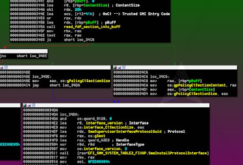
An attacker in possession of an RP2350 device, as well as access to semiconductor deprocessing equipment and a focused ion beam (FIB) system, could extract the contents of the antifuse bit cells as plaintext in a matter of days. While a FIB system is a very expensive scientific instrument (costing several hundred thousand USD, plus ongoing operating expenses in the tens of thousands per year), it is possible to rent time on one at a university lab. These costs are low enough to be well within the realm of feasibility in many scenarios given the potential value of the keys in the device.
The attack can theoretically be performed with only a single device and would take a skilled attacker approximately 1-2 weeks of work to perform the initial reverse engineering and process development on blank or attacker-programmed test chips. Actual target devices would take 1-2 days per chip to prepare the sample and extract a small amount of data such as a key; a full fuse dump might require an additional day of machine time for imaging of the entire array.
As with any invasive attack, there is a small chance of the device being damaged during handling and deprocessing, so a real-world attacker would likely procure several samples to ensure a successful extraction.
The attack is based on established semiconductor failure analysis techniques and is not specific to the RP2350; it is likely that similar techniques can be used to extract data from other devices with antifuse-based memory.
Suggested User Mitigation
Users of the RP2350 can mitigate the basic form of the attack by using a “chaffing” technique taking advantage of the paired nature of the bit cells. By using only the low half (words 0-31) or high half (words 32-63) of a page to store cryptographic keys, and storing the complement of the key in the opposite half of the page, each pair of bit cells will have exactly one programmed and one unprogrammed bit. Since the basic passive voltage contrast (PVC) technique cannot distinguish between the two bits sharing the common via, the attacker will see the entire page as being all 1s.
This mitigation does not provide complete protection, however: by taking advantage of the circuit-edit capabilities of a FIB, an attacker could likely cut or ground the word lines being used for chaffing and then use PVC to read only the key bits. We intend to explore this extended attack in the future but have not yet tested it.
Consequences
This novel attack technique of using PVC to invasively read out data from antifuse-based OTP memory calls into question the security model of any device or system, which assumes that the OTP memory cannot be read by an attacker with physical control of the device. Security models which mandate a per-device cryptographic secret are not exposed to significant additional risk, but products which have a shared cryptographic secret stored in the antifuse-based OTP memory are at substantial additional risk from the compromise of a shared secret through this invasive attack.
The simple form of the attack demonstrated here recovers the bitwise OR of two physically adjacent memory bitcell rows sharing common metal 1 contacts, however, we believe it is possible for an attacker to separate the even/odd row values with additional effort.
Furthermore, it is highly likely that all products using the Synopsys dwc_nvm_ts40* family of memory IPs on the TSMC 40nm node are vulnerable to the same attack, since the attack is not specific to the RP2350 but rather against the memory itself.
IOActive has not yet tested our technique against other vendors’ antifuse IP blocks or on other process nodes. Nonetheless, IOActive assessed it to have broad applicability to antifuse-based memories.
Additional Information
IOActive’s full disclosure report is available here. When available, a preprint paper, which has been submitted to an academic conference will be shared on the IOActive website.
Dr. Andrew Zonenberg is a keynote speaker on this topic at the Hardware Reverse Engineering Workshop (HARRIS 2025) held on 17 and 18 March 2025 in Bochum, Germany.
ACKNOWLEDGEMENTS
IOActive would like to thank the Raspberry Pi team for the excellent coordination and communication during the disclosure process.