
This is Part 1 of a 3-Part series. You can find Part 2 here and Part 3 here.
Introduction
Manufacturers of consumer electronics often use embedded security processors to authenticate peripherals, accessories, and consumables. Third parties wishing to build unlicensed products (clones) within such an ecosystem must defeat or bypass this security for their products to function correctly.
In this series, the IOActive silicon lab team will take you on a deep dive into one such product, examining both the OEM product and the clone in detail.
Fundamentally, the goal of a third party selling an unlicensed product is for the host system to recognize their product as authentic. This can be achieved by extracting key material from an OEM or licensed accessory and putting it on a new processor (difficult, but allows the third party to manufacture of an unlimited number of clones) or by recycling security processors from damaged or discarded accessories (low effort since there is no need to defeat protections on the secure element, but the number of clones is limited by the number of security chips that the third party can find and recycle). In some cases, it may also be possible to bypass the cryptographic authentication entirely by exploiting implementation or protocol bugs in the authentication handshake.
We’ll begin our analysis by comparing the security processors from an OEM and clone device to see which path was taken in this case. The first step is to locate the processors, which can be challenging since security chips tend to have deliberately confusing or nondescript markings to frustrate reverse-engineering efforts.
Package Comparison
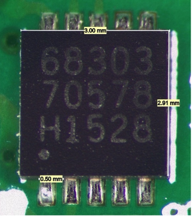
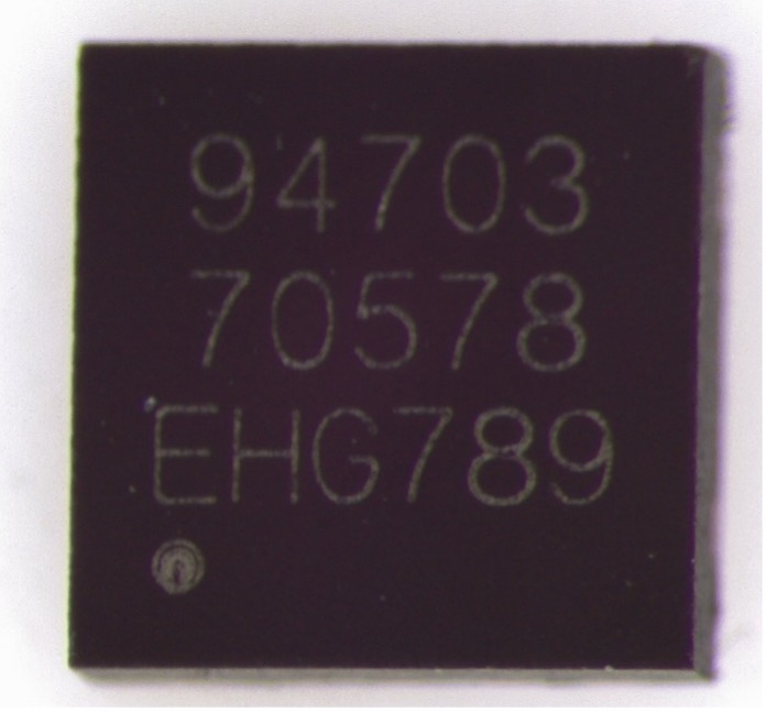
Comparing the top-side markings, we see:
- The first three digits of the first line are different.
- The second line is identical.
- The third line is completely different: three letters and three numbers on the clone versus one letter and four numbers on the OEM part.
- The font weight of the laser engraving is lighter on the clone and heavier on the OEM.
- There is no manufacturer logo marked on either device.
- The pin 1 marking dot of the OEM part has a well-defined edge, while the pin 1 marker of the clone has a small ring of discoloration around it.
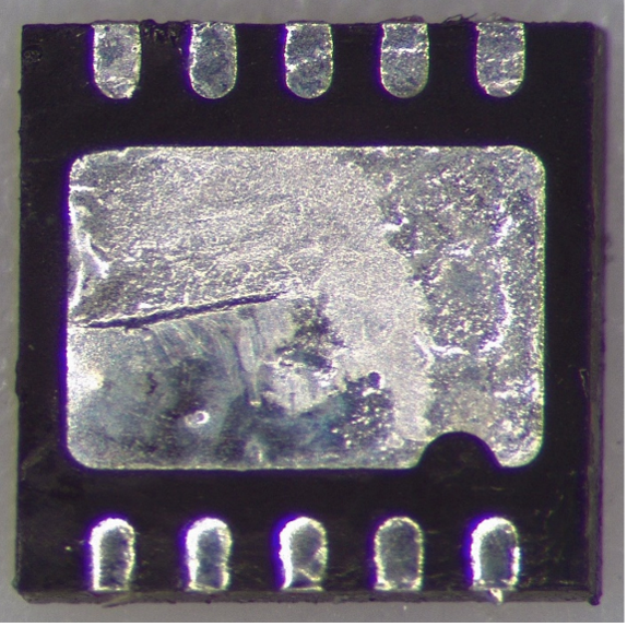
Both components are packaged in an 8-pin 0.5 mm pitch DFN with a thermal pad featuring a notch at pin 1 position. No distinction is visible between the devices from the underside.
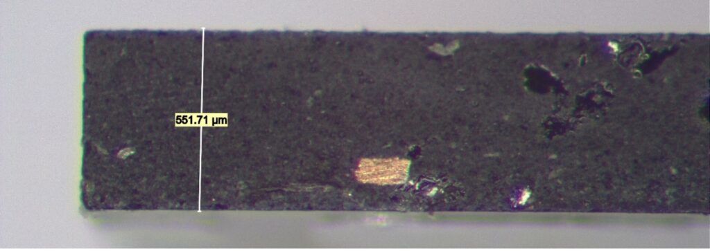
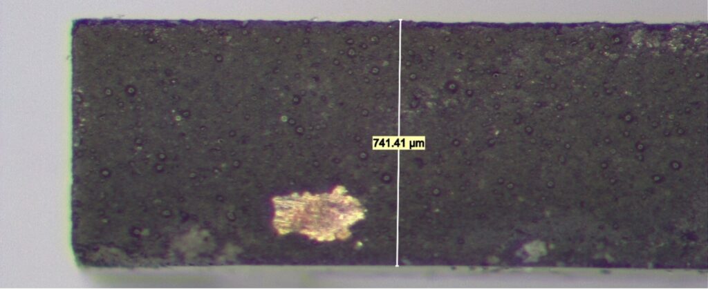
Looking from the side, we see that the clone package is significantly thicker.
Top Metal Comparison
At this stage of the analysis, it seems likely that the devices are different given the packaging variations, but this isn’t certain. Semiconductor vendors occasionally change packaging suppliers or use multiple factories to improve supply chain robustness, so it’s entirely possible that these components contain the same die but were packaged at different facilities. In order to tell for sure, we need to depackage them and compare the actual silicon.
After depackaging, the difference is obvious, even before putting the samples under the microscope. The OEM die is rectangular and about 2.6x the area of the clone die (3.24 mm2 for the OEM versus 1.28 mm2 for the clone). It also has a yellow-green tint to it, while the clone is pink.
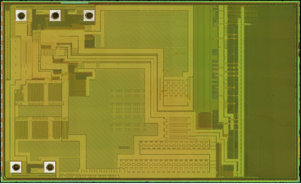
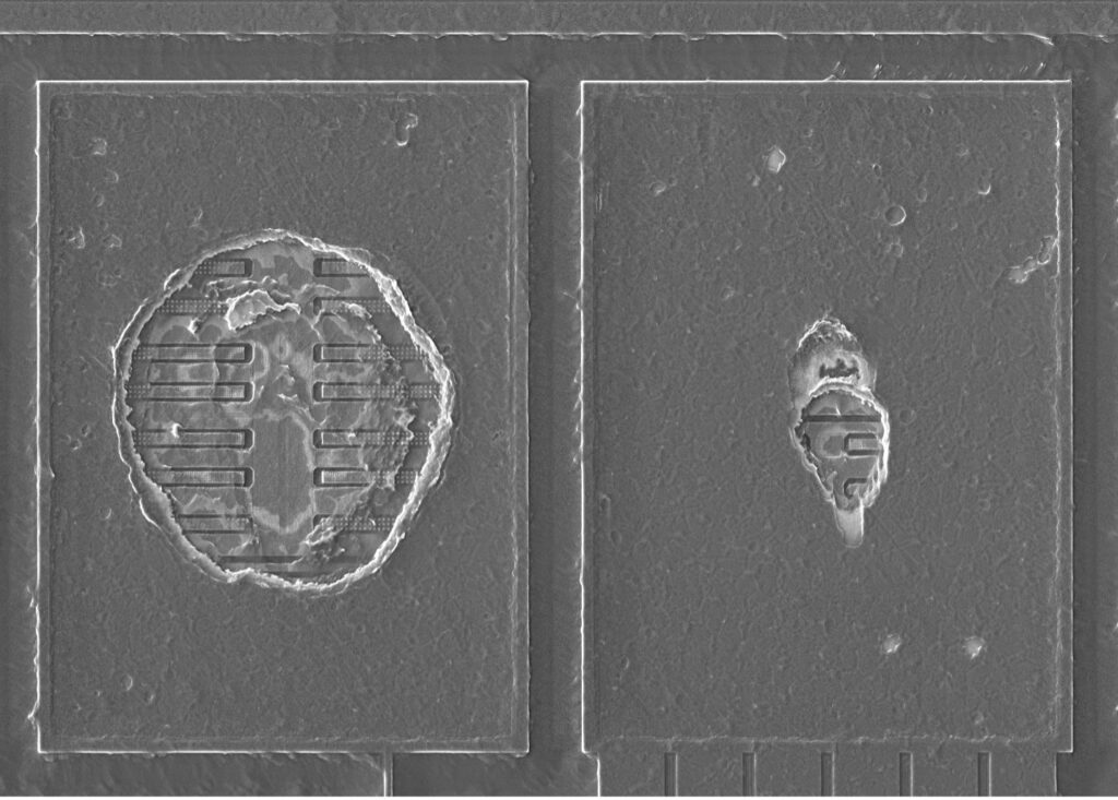
The OEM die has five gold ball bonds, three in the top left and two in the bottom left.
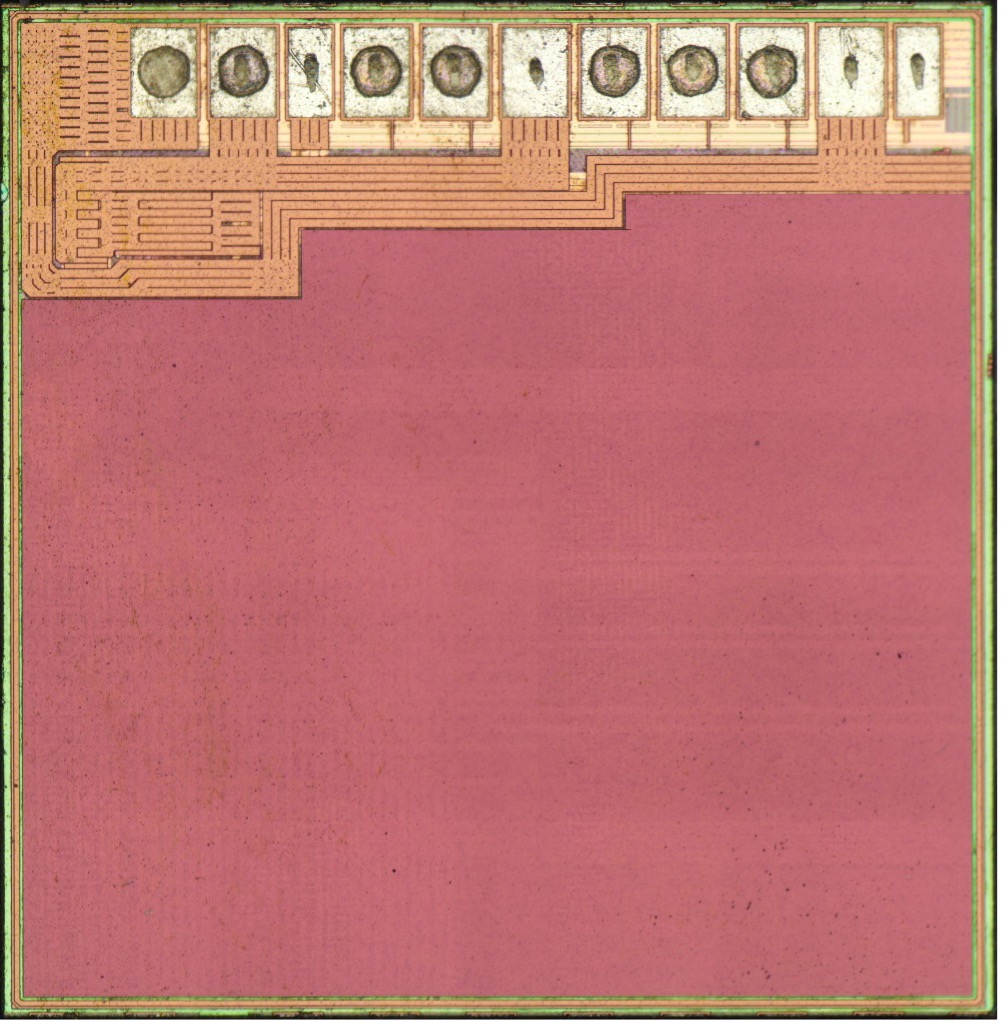
In contrast, the clone die has 11 pads along the top edge. Two are narrower than the rest and appear intended for factory test only, two redundant power/ground pads are full sized but unbonded (showing only probe scrub marks from factory test), and the remaining seven have indentations from copper ball bonds (which were chemically removed to leave a flat specimen surface).
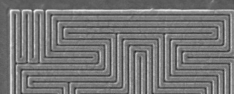
The OEM die has no evidence of an antitamper mesh; however, the surface appears to be completely covered by a dense grid of power/ground lines in-between larger high-current power distribution buses. The only exception is the far-right side, which is only covered by CMP filler (dummy metal features serving no electrical function, but which aid in manufacturability). Since sensitive data lines are not exposed on the top layer, the device is still protected against basic invasive attacks.
The clone die has large power and ground distribution buses on the top edge near the bond pads, while the remainder of the surface is covered by a fine mesh of wires clearly intended to provide tamper resistance. Typically, secure elements will fail to boot and/or erase flash if any of these lines are cut or shorted while the device is under power.
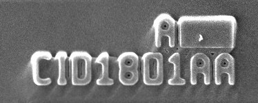
Neither die has any vendor logo or obvious identifying markings on it. The OEM part has no markings whatsoever; the clone part has mask revision markings suggesting six metal layers and a nine-digit alphanumeric ID code “CID1801AA” (which returned no hits in an Internet search).
Concluding Thoughts
The clone security processor is clearly a different device from the OEM part rather than a recycled chip. This means that the third party behind the clone must have obtained the authentication key somehow and flashed it to their own security processor.
Interestingly, the clone processor is also a secure element with obvious antitamper features! We believe that the most likely rationale is that the third party is attempting to stifle further competition in the market—they already have to share the market with the OEM but are trying to avoid additional clones becoming available.
The clone part also looks very similar to the OEM part upon casual inspection—both are packaged in the same 8-pin DFN form factor and have markings that closely resemble one another. Normally this is a sign of a counterfeit device; however, there is little chance of the OEM buying their security chip from an untrustworthy source, so it seems doubtful that the clone chip manufacturer was intending to fool the OEM into using their part. One possible explanation is that the authentication scheme was defeated by a fourth party, not the manufacturer of the clone accessory, and that they produced this device as a drop-in equivalent to the OEM security processor to simplify design of clones. Using a footprint compatible package and marking it with the same ID number would make sense in this scenario.
In the next part of this series, we’ll compare the manufacturing process technology used on the two components.