EDITORIAL, INSIGHTS | May 22, 2024

Transportation Electrification Cybersecurity Threatscape

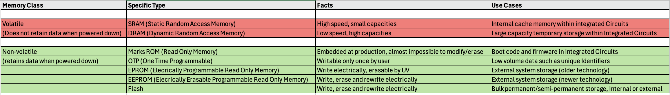
World-Wide Electric Vehicle (EV) Charging Infrastructure Trends

The global push to meet rising EV adoption with sufficient EV smart charger infrastructure is astoundingly challenging. Bloomberg estimates the global charging infrastructure market opportunity to be $1.9T between 2022 and 2050. That opportunity will be seized upon by a host of organizations large and small, public and private. From EV fleet depots to fast charging stations along highwaysparking garagessmart chargers for employees, and home chargers, EV supply equipment (EVSE) are already becoming a common sight.  The graph below depicts the world-wide cumulative global public charging connections:

World-wide trends of transition and adoption of EVs is due to climate control and carbon pollution-free electricity sector goals and policies that are being mandated over the coming years around the world, such as:

  • In the USA, Executive Order 14057[1] restricts all government agencies’ new acquisitions of light-duty vehicles to only EVs by 2027 and mid- and heavy-duty vehicle acquisitions to only EVs by 2035.
  • In California, Executive Order N-79-20[2], ends sales of ICE passenger vehicles and trucks by 2035[3].
  • The EU and UK have banned sales[4] of new combustion engine cars from 2035.

The Battery Electric Vehicle (BEV) and charging infrastructure landscape is rapidly evolving technologically and operationally in a market where cost and time-to-market are prioritized higher than security[5]. Technologies used to build the BEV ecosystem suffer from well-known cybersecurity issues, which expose vulnerabilities and risk. Current charging stations are operated as build-and-forget devices that are highly exposed and network connected, with cyber and physical vulnerabilities which pose a great challenge to the ecosystem, including bulk electric and distribution system stability, with limited current threat mitigation.

Securing such an advanced, fully connected, and heterogeneous supply grid will take a similar effort to the Information and Communication Technology (ICT) sectors that secure webservers and cloud infrastructure, and this would also include mitigations around the cyberphysical vulnerabilities unique to the BEV ecosystem.

HPC standards for the Megawatt Charging System (MCS) are being developed by the CharIN (Charging Interface Initiative eV.) international standards organization[6].

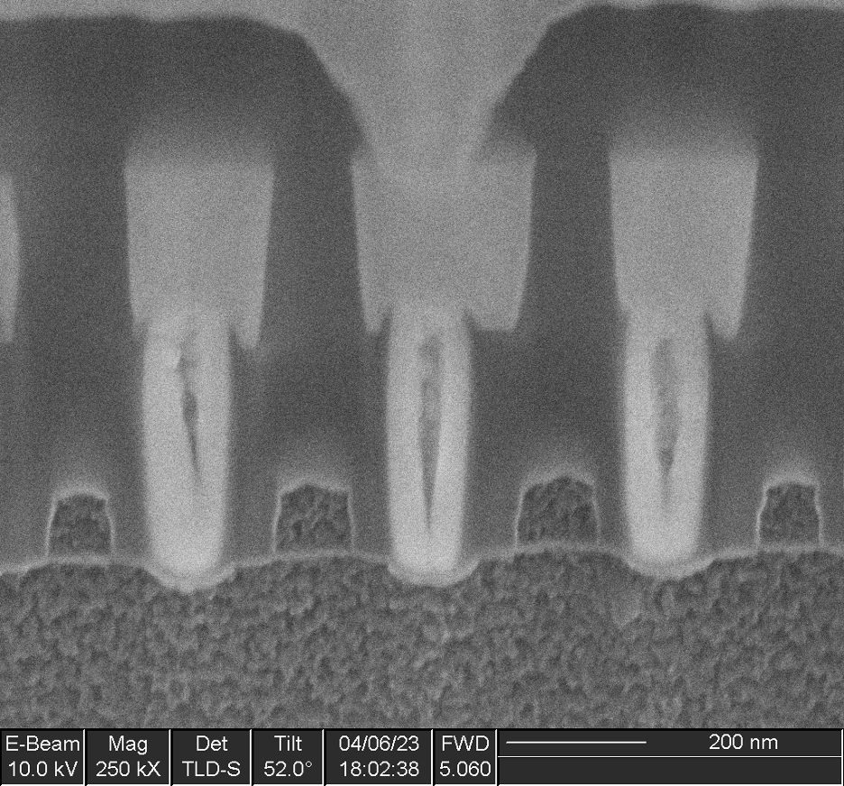
Modern electrified transportation vehicles will require a HPC infrastructure. Cybersecurity vulnerabilities in HPC systems operating at very high levels of power pose a serious cyberphysical threat to the new electric vehicles and supporting infrastructure, but also to the electrical grid (bulk and distribution) that supplies power to the HPC systems. These cyberphysical vulnerabilities will require focused, skillful mitigation.  

The potential consequences of a successful skillful attack on a BEV or ESVE system could produce remote code execution on BEVs or EVSEs, physically damaged vehicles or chargers, local or regional power outages, and larger coupling effects across countries from induced cascading failures.

IOActive’s Vehicle Cybersecurity Vulnerability Findings

In-vehicle technology is a top selling point for today’s car buyers[7]. What was once simply a “connected vehicle” is now increasingly more feature-rich, with software systems like self-driving and driver assist, complex infotainment systems, vehicle-to-other communication and integration with external AI. More than ever, all of this exciting technology turns modern vehicles into targets for malicious cyberattacks such as ransomware. It is imperative that automotive manufacturers take additional action now to infuse cybersecurity into their vehicles and mitigate potential threats. Moreover, EVSE manufacturers and utilities need to increase efforts to manage their highly impactful risks.

IOActive’s pioneering vehicle cybersecurity research began with the ground-breaking 2015 Jeep hack[8] that evolved into our ongoing vehicle research that has included commercial trucks, EVSE, and autonomous vehicles.

For over a decade, IOActive has been publishing original research blogs and papers:

EVSE Cybersecurity Incidents Are Increasing

The growing popularity of Electric Vehicles (EVs) attracts not only gas-conscious consumers but also cybercriminals interested in using EV charging stations to conduct large-scale cyberattacks for monetization purposes, espionage attacks, politically motivated attacks, theft of private/sensitive data (e.g., drivers’ data), falsifying EV ranges, and more. EVSEs, whether in a private garage or on a public parking lot, are connected IoT devices, running software that interacts with payment systems, maintenance systems, OEM back-end systems, telecommunications, and the smart grid. Therefore, charging stations pose significant cybersecurity risks.

Early incidents of cyberattacks on charging stations include the following:

EVSE cybersecurity incidents are on the increase. Links to information on several other cybersecurity hacks, as well as further reading regarding EVSE cybersecurity, are listed at the end of this blog post.

EVSE cybersecurity risk and threat scenarios include a wide variety of potential issues:

  • EVSE malware attacks threatening the integrity the electric grid/transportation network, leading to widespread disruptions in power supply and electric grid load balancing concerns
  • Ransomware attacks
  • Leakage/manipulation of sensitive data (e.g., PII, credentials, and payment card data)
  • Physical attacks to disable EVSEs, steal power, or and infect EVSEs with malware via accessible USB ports
  • Authentication RFID, NFC, or credit card chip attacks that could deny EVSE charging sessions or perform false billing
  • EVSE or grid Denial of Service attacks, impacting drivers’ ability to recharge during a hurricane or wildfire evacuation
  • Firmware/software update attacks, causing access disruption to the necessary cloud services for payment processing
  • Bypassing bootloader protections, which can allow attackers with physical access to gain root access into EVSEs to launch attacks on the backend infrastructure while appearing as a trusted device
  • An EVSE attack through the charging cable could compromise an EV, causing fire or other damage

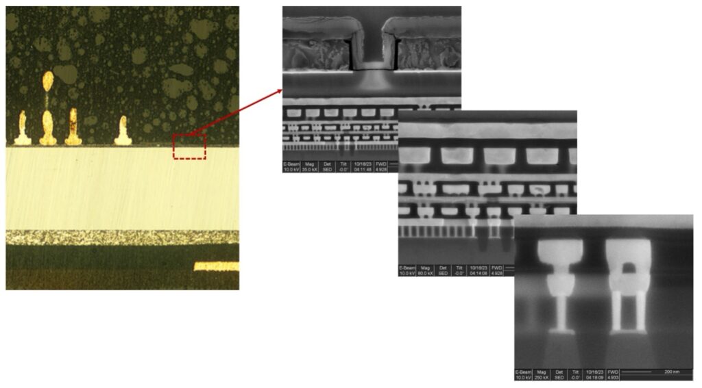
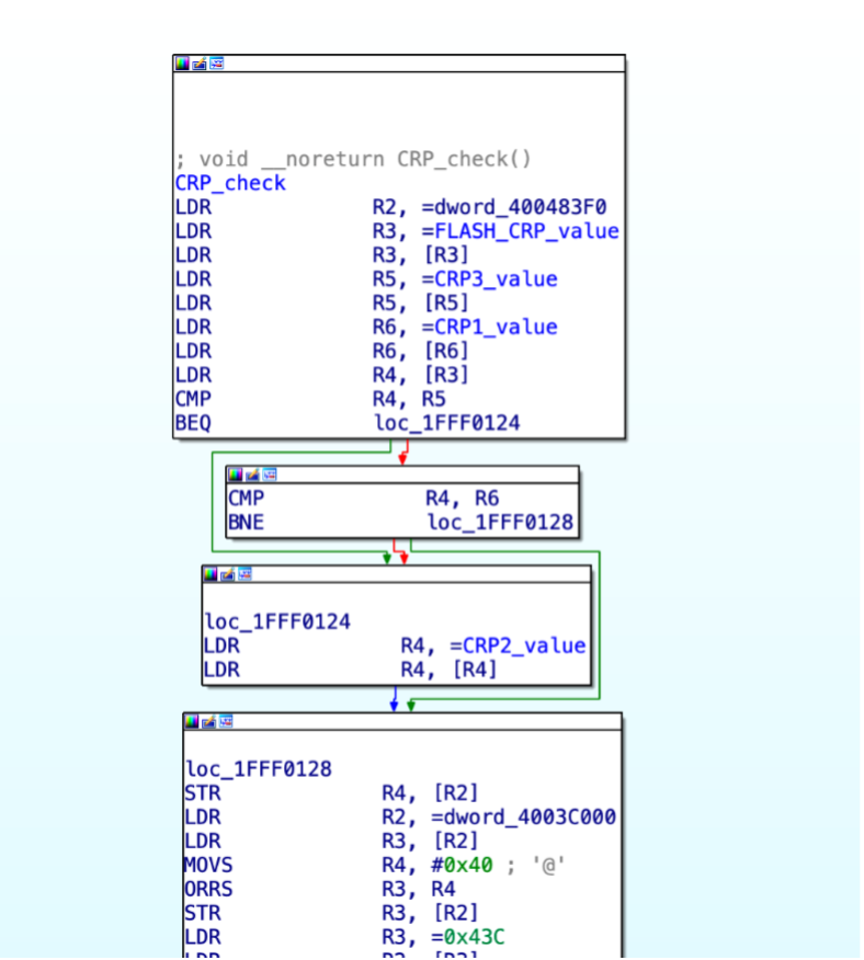
IOActive’s Electric Vehicle Charging Infrastructure Vulnerability Findings

Over the past five years, IOActive has conducted several EVSE cybersecurity penetration testing engagements for automotive and commercial truck OEMs/suppliers and EVSE vendors. Examples of IOActive’s electrification penetration testing include assessments of Level 2 EVSEs, DC Fast Chargers (DCFCs), Open Charge Point Protocol (OCPP)/cloud services, front-end/back-end web applications, onsite network configuration reviews, and EV vans.

For the past year, IOActive has led an international EVSE standards working group which has developed a public EVSE Threat Model White Paper that identifies EVSE risks, vulnerabilities, and design flaws.  The paper also includes threat scenarios ranked based on magnitude, duration, recovery effort, safety costs, effect and confidence/reputation damage. This White Paper can be shared with industry members upon request.

IOActive Welcomes Future EVSE Cybersecurity Discussions with Industry

We would like to continue to support the key industries impacted by the transition to electrified vehicles. Much of the most detailed work that we have done cannot be shared publicly. We welcome those with a need to know about the risks of and mitigations for BEVs and EVSEs to engage with us for a briefing on example extant vulnerabilities, technical threat models, threat actors, consequences of operationalized attacks, and other threat intelligence topics, as well as potential mitigations and best practices.

If you are interested in hosting IOActive for a briefing, and/or would like copies of the aforementioned presentations or white paper please contact us.

EVSE Cybersecurity Incident References:

Suggested Reading:


[1]https://www.whitehouse.gov/briefing-room/presidential-actions/2021/12/08/executive-order-on-catalyzing-clean-energy-industries-and-jobs-through-federal-sustainability/
[2]https://ww2.arb.ca.gov/resources/fact-sheets/governor-newsoms-zero-emission-2035-executive-order-n-79-20
[3]https://www.gov.ca.gov/wp-content/uploads/2020/09/9.23.20-EO-N-79-20-Climate.pdf
[4]https://www.europarl.europa.eu/topics/en/article/20221019STO44572/eu-ban-on-sale-of-new-petrol-and-diesel-cars-from-2035-explained
[5]https://www.iea.org/reports/global-ev-outlook-2023/trends-in-charging-infrastructure
[6]https://www.charin.global/
[7]https://finance.yahoo.com/news/connected-vehicle-technology-becoming-key-140000573.html
[8]https://www.wired.com/2015/07/hackers-remotely-kill-jeep-highway/

INSIGHTS, RESEARCH | May 16, 2024

Field-Programmable Chips (FPGAs) in Critical Applications – What are the Risks?

What is an FPGA?

Field-Programmable Gate Arrays (FPGAs) are a type of Integrated Circuit (IC) that can be programmed or reprogrammed after manufacturing. They consist of an array of logic blocks and interconnects that can be configured to perform various digital functions. FPGAs are commonly used in applications where flexibility, speed, and parallel processing capabilities are required, such as telecommunications, automotive, aerospace, and industrial sectors.

FPGAs are often found in products that are low volume or demand short turnaround time because they can be purchased off the shelf and programmed as needed without the setup and manufacturing costs and long lead times associated with Application-Specific Integrated Circuits (ASICs). FPGAs are also popular for military and aerospace applications due to the long lifespan of such hardware as compared to typical consumer electronics. The ability to update deployed systems to meet new mission requirements or implement new cryptographic algorithms—without replacing expensive hardware—is valuable.

These benefits come at a cost, however: additional hardware is required to enable reprogramming. An FPGA-based design will use many more transistors than the same design implemented as an ASIC, increasing power consumption and per-device costs.

Implementing a circuit with an FPGA vs an ASIC can also come with security concerns. FPGA designs are compiled to a “bitstream,” a digital representation of the circuit netlist, which must be loaded into the FPGA for it to function. While bitstream formats are generally undocumented by the manufacturer, several projects are working towards open-source toolchains (e.g., Project X-Ray for the Xilinx 7 series) and have reverse engineered the bitstream formats for various devices.

FPGA bitstreams can be loaded in many ways, depending on the FPGA family and application requirements:

  • Serial or parallel interfaces from an external processor
  • JTAG from a debug cable attached to a PC
  • Serial or parallel interfaces to an external flash memory
  • Separate stacked-die flash memory within the same package as the FPGA
  • Flash or One-Time-Programmable (OTP) memory integrated into the FPGA silicon itself

In this post, we will focus on Xilinx because it was the first company to make a commercially viable FPGA back in 1985 and continues to be a world leader in the field. AMD acquired Xilinx in 2020 in a deal worth $60 billion, and today they control over 50% of the world’s programmable logic chips.

The Spartan™ 6 family of Xilinx FPGAs offers low-cost and low-power solutions for high-volume applications like displays, military/emergency/civil telecommunications equipment, and wireless routers. Spartan 6 was released in 2009, so these chips are relatively low-tech compared with their successors, the Spartan 7 and Xilinx’s higher end solutions (e.g., the Zynq and Versal families).

The Spartan 6 bitstream format is not publicly known, but IOActive is aware of at least one research group with unreleased tooling for it. These devices do not contain internal memory, so the bitstream must be provided on external pins each time power is applied and is thus accessible for an attacker to intercept and potentially reverse engineer.

FPGA vendors are, of course, aware of this risk and provide security features, such as allowing bitstreams to be encrypted on external flash and decrypted on the FPGA. In the case of the Spartan 6 family, the bitstream can be encrypted with AES-256 in CBC mode. The key can be stored in either OTP eFuses or battery-backed Static Random Access Memory (SRAM), which enables a self-destruct function where the FPGA can erase the key if it detects tampering.

The AES block used in the Spartan 6, however, is vulnerable to power analysis, and a team of German researchers developed a successful attack against it: “On the Portability of Side-Channel Attacks – An Analysis of the Xilinx Virtex 4, Virtex 5, and Spartan 6 Bitstream Encryption Mechanism.”

An example of a Xilinx Spartan 6 application is the Russian military radio R-187-P1 made by Angstrem, so we decided to use this as our test case.

AZART R-187-P1 Product Overview

Since its release in 2012, several researchers have discovered that the radio provides built-in protocols to allow communication across multiple standards, including older analogue Russian radios, UAV commands, and even TETRA. While the advertised frequency range is 27 to 520 MHz, recent firmware updates enabled a lower range of frequencies down to 100 kHz with AM.  

The features of this radio are fairly well known. The following was posted by @SomeGumul, a Polish researcher, on Twitter/X:

The trophy in the form of the Russian radio station “Azart”, announced by the Russians as a “native, Russian” sixth-generation device for conducting encrypted conversations, works on American radio components. The basis of the encryption system is, in particular, the Spartan®-6 FPGA (field-programmable gate array) system.  It is produced by the American company XILINX (AMD) in Taiwan.

Ironically, despite being advertised as the forefront of Russia’s military technical prowess, the heart of this device was revealed by Ukrainian serviceman Serhii Flash (Сергей Флэш) to be powered by the Spartan 6 FPGA. This FPGA is what enables the handheld radio’s capabilities to be redefined by mere software updates, allowing its users to speak over virtually any radio standard required—past, present, or future. While most of the currently implemented protocols are unencrypted to allow backward compatibility with other older, active service equipment, communication between two AZART radios enables frequency hopping up to 20,000 frequencies per second. This high rate of frequency hopping creates challenges for eavesdropping and position triangulation. The radio’s implementation of TETRA also supports encryption with the inclusion of a supporting radio trunk, where the radio is referred to as being in Trunked Mode Operation (TMO). Otherwise, while in Direct Mode Operation (DMO), the radio only supports voice scrambling in the time and frequency domains.   

20,000 frequency hops per second is quite a feat for a radio. Extremely precise timing is required for two or more radios to sync across hops and still communicate clearly. This timing source is gained wirelessly from GPS and GLONASS. As such, this advanced feature can be disabled simply by jamming GPS frequencies.

While this attack may be sufficient, GPS signals are ubiquitous and neutral sources of precise timing that are often required by both sides of any conflict. So, while jamming the frequencies may work in a pinch, it would be cleaner to find a solution to track this high rate of frequency hopping without having to jam a useful signal. To find this solution, we must investigate the proprietary Angstrem algorithm that drives the pseudo-random frequency hopping. To do this, we begin by looking at the likely driver: the Spartan 6 FPGA.

Chipset Overview

It is currently unknown if the Spartan 6 on the AZART is utilizing an encrypted bitstream; however, due to its wartime purpose, it must not be ruled out. While waiting for the procurement of a functioning radio, IOActive began a preliminary investigation into the functioning of the Spartan 6 with a specific focus on areas related to encryption and decryption of the bitstream.

Mainboard of AZART Highlighting the Spartan 6

At the time of writing this post, the XC6SLX75-3CSG484I sells for around $227 from authorized US distributors; however, it can be obtained for much lower prices in Asian markets, with sellers on AliExpress listing them for as low as $8.47. While counterfeits are prevalent in these supply chains, legitimate parts are not difficult to obtain with a bit of luck.

In addition to the FPGA, one other notable component visible on the board is the Analog Devices TxDAC AD9747, a dual 16-bit 250 Msps Digital-to-Analog Converter (DAC) intended for SDR transmitters. Assuming this is being used to transmit I/Q waveforms, we can conclude that the theoretical maximum instantaneous bandwidth of the radio is 250 MHz, with the actual bandwidth likely being closer to 200 MHz to minimize aliasing artifacts.

Device Analysis

IOActive procured several Spartan 6 FPGAs from a respected supplier for a preliminary silicon teardown to gain insight into how the chip handles encrypted bitstreams and identify any other interesting features. As a standalone package, the Spartan chip looks like this:

The CSG484 package that contains the Spartan 6 is a wire-bonded Ball-Grid Array (BGA) consisting of the IC die itself (face up), attached by copper ball bonds to a four-layer FR4 PCB substrate and overmolded in an epoxy-glass composite. The substrate has a grid of 22×22 solder balls at 0.8 mm pitch, as can be seen in the following cross section. The solder balls are an RoHS-compliant SAC305 alloy, unlike the “defense-grade” XQ6SLX75, which uses Sn-Pb solder balls. The choice of a consumer-grade FPGA for a military application is interesting, and may have been driven by cost or component availability issues (as the XQ series parts are produced in much lower volume and are not common in overseas supply chains).

Spartan 6 Cross Section Material Analysis

The sample was then imaged in an SEM to gain insight into the metal layers for to order to perform refined deprocessing later. The chip logic exists on the surface of the silicon die, as outlined by the red square in the following figure.

Close-up of FPGA Metal Layers on Silicon Die

The XC6SLX75 is manufactured by Samsung on a 45 nm process with nine metal layers. A second FPGA was stripped of its packaging for a top-down analysis, starting with metal layer nine.

Optical Overview Image of Decapsulated Die Xilinx XC6SLX75

Looking at the top layer, not much structure is visible, as the entire device is covered by a dense grid of power/ground routing. Wire bond pads around the perimeter for power/ground and I/O pins can clearly be seen. Four identical regions, two at the top and two at the bottom, have a very different appearance from the rest of the device. These are pairs of multi-gigabit serial transceivers, GTPs in Xilinx terminology, capable of operation at up to 3.2 Gbps. The transceivers are only bonded out in the XC6SLX75T; the non –T version used in the radio does not connect them, so we can ignore them for the purposes of this analysis.

The metal layers were then etched off to expose the silicon substrate layer, which provides better insight into chip layout, as shown in the following figure.

Optical Overview Image of Floorplan of Die Xilinx XC6SLX75

After etching off the metal and dielectric layers, a much clearer view of the device floorplan becomes visible. We can see that the northwest GTP tile has a block of logic just south of it. This is a PCIe gen1 controller, which is not used in the non –T version of the FPGA and can be ignored.

The remainder of the FPGA is roughly structured as columns of identical blocks running north-south, although some columns are shorter due to the presence of the GTPs and PCIe blocks. The non-square logic array of Spartan 6 led to poor performance as user circuitry had to be shoehorned awkwardly around the GTP area. Newer-generation Xilinx parts place the GTPs in a rectangular area along one side of the device, eliminating this issue.

The light-colored column at the center contains clock distribution buffers as well as Phase-Locked Loops (PLLs) and Digital Clock Managers (DCMs) for multiplying or dividing clocks to create different frequencies. Smaller, horizontal clock distribution areas can be seen as light-colored rows throughout the rest of the FPGA.

There are four columns of RAM containing a total of 172 tiles of 18 kb, and three columns of DSP blocks containing a total of 132 tiles, each consisting of an 18×18 integer multiplier and some other logic useful for digital signal processing. The remaining columns contain Configurable Logic Blocks (CLBs), which are general purpose logic resources.

The entire perimeter of the device contains I/O pins and related logic. Four light-colored regions of standard cell logic can be seen in the I/O area, two on each side. These are the integrated DDR/DDR2/DDR3 Memory Controller Blocks (MCBs).

The bottom right contains two larger regions of standard cell logic, which appear related to the boot and configuration process. We expect the eFuse and Battery-Backed SRAM (BBRAM), which likely contain the secrets required to decrypt the bitstream, to be found in this area. As such, this region was scanned in high resolution with the SEM for later analysis.

SEM Substrate Image of Boot/AES Logic Block 1

Utilizing advanced silicon deprocessing and netlist extraction techniques, IOActive hopes to refine methodologies for extracting the configured AES keys required to decrypt the bitstream that drives the Spartan 6 FPGA.

Once this is complete, there is a high probability that the unencrypted bitstream that configures the AZART can be obtained from a live radio and analyzed to potentially enumerate the secret encryption and frequency hopping algorithms that protect the current generation of AZART communications. We suspect that we could also apply this technique to previous generations of AZART, as well as other FPGA-based SDRs like those commonly in use by law enforcement, emergency services, and military operations around the world.

INSIGHTS, RESEARCH | May 15, 2024

Evolving Cyber Threatscape: What’s Ahead and How to Defend

The digital world is a dangerous place. And by all accounts, it’s not getting a whole lot better.

Damages from cybercrime will top a staggering $8 trillion this year, up from an already troubling $1 trillion just five years ago and rocketing toward $14 trillion by 2028. Supply chains are becoming juicier targets, vulnerabilities are proliferating, and criminals with nation-state support are growing more active and more sophisticated. Ransomware, cryptojacking, cloud compromises, and AI-powered shenanigans are all on a hockey-stick growth trajectory.

Looking ahead, there are few sure things in infosec other than the stone-cold, lead-pipe lock that systems will be hacked, data will be compromised, money will be purloined, and bad actors will keep acting badly.

Your organization needn’t be a victim, however. Forewarned is forearmed, after all.

Here’s what to expect in the evolving cyber threatscape over the next 12 to 18 months along with some steps every security team can take to stay secure in this increasingly hostile world.

The Weaponization of AI

The Threat: The coming year promises to be a big one for exploiting the ability of AI (artificial intelligence) and Large Language Models (LLMs) to spew misinformation, overwhelm authentication controls, automate malicious coding, and spawn intelligent malware that proactively targets vulnerabilities and evades detection. Generative AI promises to empower any attacker — even those with limited experience or modest resources — with malicious abilities previously limited to experienced users of frameworks like Cobalt Strike or Metasploit.

Expect to see at least some of these new, nefarious generative AI tools offered as a service through underground criminal syndicates, broadening the global cabal of troublesome threat actors while expanding both the population and the richness of available targets. The steady increase in Ransomware-as-a-Service is the clearest indicator to date that such criminal collaboratives are already on the rise.

Particularly ripe for AI-enabled abuse are social engineering-based operations like phishing, business email compromise, and so-called “pig butchering” investment, confidence and romance scams. Generative AI is eerily adept at turning out convincing, persuasive text, audio, and video content with none of the spelling, grammar, or cultural errors that traditionally made such hack attempts easy to spot. Add the LLMs ability to ingest legitimate business communications content for repurposing and translation and it’s easy to see how AI will soon be helping criminals craft super-effective global attacks on an unprecedented scale.

The Response: On a positive note, AI, as it turns out, can play well on both sides of the ball: offense and defense.

AI is already proving its worth, bolstering intelligent detection, response, and mitigation tools. AI-powered security platforms can analyze, model, learn, adapt, and act with greater speed and capacity than any human corps of security analysts ever could. Security professionals need to skill-up now on the techniques used to develop AI-powered attacks with the goal of creating equally innovative and effective mitigations and controls.

And because this new generation of smart malware will make the targeting of unmitigated vulnerabilities far more efficient, the basic infosec blocking and tackling — diligent asset inventory, configuration management, patching — will be more critical than ever.

Clouds Spawn Emerging Threats

The Threat: Business adoption of cloud computing technology has been on a steady rise for more than a decade. The current macroeconomic climate, with all of its challenges and uncertainty, promises to accelerate that trend for at least the next few years. Today, more than four in ten enterprises say they are increasing their use of cloud-based products and services and about one-third plan to continue migrating from legacy software to cloud-based tools this year. A similar share is moving on-premises workloads in the same direction.

Good for business. However, the cloud transformation revolution is not without its security pitfalls.

The cloud’s key benefits — reduced up-front costs, operational vs. capital expenditure, improved scalability and efficiency, faster deployment, and streamlined management — are counterbalanced by cloud-centric security concerns. The threatscape in the era of cloud is dotted with speed bumps like misconfigurations, poor coding practices, loose identity and access controls, and a pronounced lack of detailed environmental visibility. All of this is compounded by a general dearth of cloud-specific security expertise on most security teams.

One area to watch going forward: Better than half of enterprise IT decision-makers now describe their cloud strategy as primarily hybrid cloud or primarily multi-cloud. Three-quarters use multiple cloud vendors. Criminals are taking note. Attacks targeting complex hybrid and multi-cloud environments — with their generous attack surface and multiple points of entry — are poised to spike.

The recent example of a zero-day exploited by Chinese hackers that allowed rogue code execution on guest virtual machines (VMs) shows that attacks in this realm are getting more mature and potentially more damaging. Threat actors are targeting hybrid and multi-cloud infrastructure, looking for ways to capitalize on misconfigurations and lapses in controls in order to move laterally across different cloud systems.

Another area of concern is the increased prevalence of serverless infrastructure in the cloud. The same characteristics that make serverless systems attractive to developers — flexibility, scalability, automated deployment — also make them irresistible to attackers. Already there’s been an uptick in instances of crypto miners surreptitiously deployed on serverless infrastructure. Though serverless generally presents a smaller attack surface than hybrid and multi-cloud infrastructure, giving up visibility and turning over control of the constituent parts of the infrastructure to the cloud service provider (CSP) raises its own set of security problems. Looking ahead, nation-state backed threat actors will almost certainly ramp up their targeting of serverless environments, looking to take advantage of insecure code, broken authentication, misconfigured assets, over-privileged functions, abusable API gateways, and improperly secured endpoints.

The Response: The best advice on securing modern cloud environments in an evolving threatscape begins with diligent adherence to a proven framework like the Center for Internet Studies’ Critical Security Controls (CIS Controls V8) and the CIS’s companion Cloud Security Guide. These prioritized safeguards, regularly updated by an engaged cadre of security community members, offer clear guidance on mitigating the most prevalent cyber-attacks against cloud-based systems and cloud-resident data. As a bonus, the CIS Controls are judiciously mapped to several other important legal, regulatory, and policy frameworks.

Beyond that fundamental approach, some steps cloud defenders can take to safeguard the emerging iterations of cloud infrastructure include:

  • Embracing the chaos: The big challenge for security teams today is less about current configurations and more about unwinding the sins of the past. Run a network visualization and get arms around the existing mess of poorly managed connections and policy violations. It’s a critical first step toward addressing critical vulnerabilities that put the company and its digital assets at risk.
  • Skilling Up: Most organizations rely on their existing networking and security teams to manage their expanding multi-cloud and hybrid IT environments. It’s a tall order to expect experts in more traditional IT to adapt to the arcana of multi-cloud without specific instruction and ongoing training. The Cloud Security Alliance offers a wealth of vendor-agnostic training sessions in areas ranging from cloud fundamentals, to architecture, auditing and compliance.
  • Taking Your Share of Shared Responsibility: The hierarchy of jurisdiction for security controls in a cloud environment can be ambiguous at best and confusing at worst. Add more clouds to the mix, and the lines of responsibility blur even further. While all major cloud providers deliver some basic default configurations aimed at hardening the environment, that’s pretty much where their burden ends. The client is on the hook for securing their share of the system and its data assets. This is especially true in multi-cloud and hybrid environments where the client organization alone must protect all of the points where platforms from various providers intersect. Most experts agree the best answer is a third-party security platform that offers centralized, consolidated visibility into configurations and performance.
  • Rethinking networking connections: Refactoring can move the needle on security while conserving the performance and capabilities benefits of the cloud. Consider the “minimum viable network” approach, a nod to how cloud can, in practice, turn a packet-switched network into a circuit-switched one. The cloud network only moves packets where users say they can move. Everything else gets dropped. Leveraging this eliminates many security issues like sniffing, ARP cache poisoning, etc. This application-aware schema calls for simply plugging one asset into another, mapping only the communications required for that particular stack, obviating the need for host-based firewalls or network zones.

    Once defenders get comfortable with the minimum viable network concept, they can achieve adequate security in even the most challenging hybrid environments. The trick is to start simple and focus on reducing network connections down to the absolute minimum of virtual wires.

Supply Chains in the Crosshairs

The Threat: Because they’re such a central component in a wide variety of business operations — and because they feature complex layers of vendor, supplier, and service provider relationships — supply chains remain a tempting target for attackers. And those attackers are poised to grow more prolific and more sophisticated, adding to their prominence in the overall threatscape.

As global businesses become more dependent on interconnected digital supply chains, the compromise of a single, trusted software component in that ecosystem can quickly cascade into mayhem. Credential theft, malicious code injection, and firmware tampering are all part of the evolving supply-chain threat model. Once a trusted third party is compromised, the result is most often data theft, data wiping, or loss of systems availability via ransomware or denial of service attack. Or all of the above.

Prime examples include the 2020 SolarWinds hack, in which government-backed Russian attackers inserted malicious code into a software update for SolarWinds popular Orion IT monitoring and management platform. The compromise went undetected for more than a year, even as SolarWinds and its partners continued serving up malicious code to some 30,000 private companies and government agencies. Many of those victims saw their data, systems and networks compromised by the backdoor buried in the bad update before the incident was finally detected and mitigated.

More recently, in the summer of 2023, attackers leveraged a flaw in Progress Software’s widely used MOVEit file transfer client, exposing the data of thousands of organizations and nearly 80 million users. In arguably the largest supply-chain hack ever recorded, a Russian ransomware crew known as Clop leveraged a zero-day vulnerability in MOVEit to steal data from business and government organizations worldwide. Victims ranged from New York City’s public school system, the state of Maine, and a UK-based HR firm serving major clients such as British Airways and the BBC.

The Response: Given the trajectory, it’s reasonable to assume that supply chain and third-party attacks like the MOVEit hack will grow in both frequency and intensity as part of the threatscape’s inexorable evolution. This puts the integrity and resilience of the entire interconnected digital ecosystem at grave and continuing risk.

To fight back, vendor due diligence (especially in the form of formal vendor risk profiles) is key. Defenders will need to take a proactive stance that combines judicious and ongoing assessment of the security posture of all the suppliers and third-party service providers they deal with. Couple that with strong security controls — compensating ones, if necessary — and proven incident detection and response plans focused on parts of the environment most susceptible to third-party compromise.

These types of attacks will happen again. As the examples above illustrate, leveraging relevant threat intelligence on attack vectors, attacker techniques, and emerging threats should feature prominently in any scalable, adaptable supply chain security strategy.

Dishonorable Mentions

The cybersecurity threatscape isn’t limited to a handful of hot-button topics. Watching the threat environment grow and change over time means keeping abreast of many dozens of evolving risk factors, attack vectors, hacker techniques and general digital entropy. Some of the other issues defenders should stay on top of in this dynamic threat environment include:

  • Shifting DDos targets: Distributed denial-of-service attacks are as old as the internet itself. What’s new is the size and complexity of emerging attacks which are now more frequently targeting mobile networks, IoT systems and Operational Technology/Industrial Control Systems (OT/ICS) that lie at the heart of much critical infrastructure.
  • Disinfo, misinfo and “deep fakes”: A product of the proliferation of AI, bad-faith actors (and bots that model them) will churn out increasing volumes of disingenuous data aimed at everything from election interference to market manipulation.
  • Rising hacktivism: Conflicts in Ukraine and Israel illustrate how hacker collabs with a stated political purpose are ramping up their use of DDoS attacks, Web defacements and data leaks. The more hacktivism cyber attacks proliferate — and the more effective they appear — the more likely nation-states will jump in the fray to wreak havoc on targets both civilian and military.
  • Modernizing malware code: C/C++ has long been the lingua franca of malware. But that is changing. Looking to harness big libraries, easier integration, and a more streamlined programming experience, the new breed of malware developers is turning to languages like Rust and Go. Not only are hackers able to churn their malicious code faster to evade detection and outpace signatures, but the malware they create can be much more difficult for researchers to reverse engineer as well.
  • Emerging quantum risk: As the quantum computing revolution inches ever closer, defenders can look forward to some significant improvements to their security toolkit. Like AI, quantum computing promises to deliver unprecedented new capabilities for threat intelligence gathering, vulnerability management, and DFIR. But also like AI, quantum has a dark side. Quantum computers can brute force their way through most known cryptographic algorithms. Present-day encryption and password-based protections are likely to prove woefully ineffective in the face of a quantum-powered attack.

Taking Stock of a Changing Threatscape

Yes, the digital world is a dangerous place, and the risks on the horizon of the threatscape can seem daunting. Navigating this challenging terrain forces security leaders to prioritize strong, scalable defenses, the kind that can adapt to emerging technology threats and evolving attack techniques all at once. It’s a multi-pronged approach.

What does it take? Adherence to solid security frameworks, judicious use of threat intelligence, updated response plans, and even tactical efforts like mock drills, penetration tests, and red team exercises can play a role in firming up security posture for an uncertain future.

Perhaps most importantly, fostering a culture of security awareness and training within the organization can be vital for preventing common compromises, from phishing and malware attacks to insider threats, inadvertent data leaks, and more.

Surviving in the evolving cyber threatscape comes down to vigilance, adaptability, and a commitment to constant learning. It’s a daunting task, but with a comprehensive, forward-thinking strategy, it’s possible to stay ahead of the curve.

INSIGHTS | May 9, 2024

Always Updated Awards 2024 Blog

We are excited to announce that IOActive received multiple prestigious awards wins this year! Keep this blog bookmarked to always stay up-to-date on the company’s accomplishments throughout 2024.

Last updated September 30, 2024

IOActive was honored for its ability to maximize security investments and enhance clients’ overall security posture and business resilience. Unlike many organizations that default to defensive strategies, we at IOActive go beyond standard penetration testing to provide clients with red and purple team services that exceed typical assessments. We prioritize a comprehensive understanding of cyber adversaries through custom adversary emulation and ethical real-world attack simulations to develop robust, secure frameworks.

“We’re delighted to win awards in multiple categories throughout 2024,” said Jennifer Sunshine Steffens, CEO at IOActive. “These awards emphasize our nearly 30 years of leadership providing unique ‘attacker’s perspective’ methodologies that drive our research-fueled approach to security services trusted by Fortune 1000 companies worldwide.”

IOActive sets itself apart from the competition by bringing a unique attacker’s perspective to every client engagement, in order to maximize security investments and improve client’s overall security posture and business resiliency.

While many organizations focus on defense by ‘default,’ IOActive’s approach encourages secure-by-design practices and policies by introducing businesses to  an attacker’s mindset so that they can better understand the threat landscape.

Understanding our adversaries is crucial. Therefore, our penetration teams surpass standard penetration testing to offer our clients a range of red and blue team solutions that go beyond traditional approaches.

Check out our secured awards below:

2024 Corporate Excellence Awards

Best Research-Led Security Services Provider 2024 – USA

IOActive is a proud winner of this year’s ‘Best Research-Led Security Services Provider 2024 – USA’ through the implementation of up-to-date research embedded in the delivery of services. The Corporate Excellence Awards ‘showcase the companies and individuals that are committed to innovation, business growth, and providing the very best products and services to clients across a wide range of industries.’

2024 Cyber Security Excellence Awards

Pen Test Team of the Year

IOActive’s penetration testing team sets itself apart from the competition by bringing a unique attacker’s perspective to every client engagement in order to maximize security investments and improve client’s overall security posture and business resiliency.

Cybersecurity Team of the Year

At IOActive, our team provides more than traditional penetration testing. We freely share our security expertise through a range of offerings including red and purple team exercises, attack simulations, security consultancy, and our highly specialized technical and programmatic services.

In addition, our leaders and consultants, spearheaded by CEO Jennifer Sunshine Steffens, have

served long tenures in the cybersecurity field and are highly skilled in research, strategic security services, risk management, quality assurance, and regulatory requirements.

Cybersecurity Provider of the Year

IOActive is a worldwide leader in research-fueled security services implementing unique “attacker’s perspective” methodologies that form the foundation of the company’s global service offerings.

Whether our customers need guidance, on-the-ground penetration testing, or the assistance of a virtual CISO, we are committed to assuring client satisfaction.

We constantly strive to develop new ways to assist our customers in handling today’s complex threatscape and long component lifecycles. Every client engagement is tailored to maximize security investments and improve overall security postures and business resiliency.

2024 Global Infosec Awards

Trailblazing Cybersecurity Service Provider

Our team has conducted groundbreaking research within a variety of industries, including research into the Boeing airplane’s network, uncovering vehicle vulnerabilities by hacking into a Jeep, a card shuffler machine and much more.

Our security services, spanning across the silicon and hardware-based levels to real-world attack simulations, demonstrate our expertise in ensuring organizations achieve security resilience.

Just as each cyberattacker and threat is different, we ensure our services are tailored to the needs of our clients – and we take pride in exceeding expectations, every time.

Trailblazing Cybersecurity Research

Our diverse cybersecurity team, with a presence in over 30 countries worldwide, combines decades of experience with cutting-edge research to develop innovative security solutions suitable for a broad range of industries and companies.

We count Fortune 1000 organizations among our customers, and we provide research-backed services across industries including automotive, medical devices, aviation, and satellite communications. Overall, we are deeply committed to offering unrelenting value and support internationally and to all of our customers.

INSIGHTS, RESEARCH | May 2, 2024

Untested Is Untrusted: Penetration Tests and Red Teaming Key to Mature Security Strategy

Organizations need to know how well their defenses can withstand a targeted attack. Red team exercises and penetration tests fit the bill, but which is right for your organization?

Information security at even well-defended enterprises is often a complex mesh of controls, policies, people, and point solutions dispersed across critical systems both inside and outside the corporate perimeter. Managing that murky situation can be challenging for security teams, many of whom are understaffed and forced to simply check as many of the boxes as they can on the organization’s framework of choice and hope for the best.

Even in a known hostile climate replete with ransomware, sophisticated bad actors, and costly data breaches, security teams are often pressured to deploy tools, coordinate with disparate IT teams, then left to stand guard: monitoring, analyzing, patching, responding, and recovering.

This largely reactive posture is table stakes for most defenders, but on its own, it leaves one important question hanging. How well will all these defenses work when bad guys come calling? Like an orchestra of talented musicians that have never had a dress rehearsal, or a well-conditioned team of athletes that have never scrimmaged, it’s difficult to know just how well the group will perform under real-world conditions. In information security in particular, organizations are often unsure if their defenses will hold in an increasingly hostile world–a world with endless vulnerabilities, devastating exploits, and evolving attackers with powerful tools and expanding capabilities.

Security’s Testing Imperative

At its heart, effective security infrastructure is a finely engineered system. Optimizing and maintaining that system can benefit greatly from the typical engineer’s inclination to both build and test.  From bird feeders to bridges, sewing machines to skyscrapers, no industrial product survives the journey from design to production without being pushed to its limits – and beyond – to see how it will fare in actual use. Tensile strength, compressive parameters, shear forces, thermal capacity, points of failure, every potential weakness is fair game. The concept of stress testing is common in every engineering discipline. Security should be no exception.

Security systems aren’t subjected to blistering heat, abrasive friction, or crushing weight, of course. But the best ones are regularly probed, prodded, and pushed to their technical limits. To accomplish this, organizations turn to one of two core testing methodologies: the traditional penetration test, and the more robust red team exercise. Both penetration testing and red teaming are proven, well-documented approaches for establishing the effectiveness of an organization’s defenses,

Determining which one is best for a particular organization comes down to understanding how penetration tests and red team exercises work and how they differ in practice, core purpose, and scope.

Penetration Testing: Going Beyond Vulnerability Assessment

Penetration Tests (“pentests” for short) are a proactive form of application and infrastructure security evaluation in which an ethical hacker is authorized to scan an organization’s systems to discover weaknesses that could lead to compromise or a data breach.   The pentester’s objectives are to identify vulnerabilities in the client environment, exploit them to demonstrate the vulnerability’s impact, and document the findings.

Penetration testing is generally considered the next step up from traditional vulnerability assessments. Vulnerability assessments – usually the product of software-driven, automated scanning and reporting – expose many unaddressed weaknesses by cross-referencing the client’s systems and software with public lists of known vulnerabilities. Penetration testing takes the discipline a step further, adding the expert human element in order to recreate the steps a real cybercriminal might take to compromise systems. Techniques such as vulnerability scanning, brute-force password attacks, web app exploitation, and social engineering can be included in the test’s stated parameters.

Penetration tests are more targeted and deliver a more accurate list of vulnerabilities present than a vulnerability assessment. Because exploitation is often included, the pentest shows client organizations which vulnerabilities pose the biggest risk of damage, helping to prioritize mitigation efforts. Penetration tests are usually contracted with strict guidelines for time and scope — and because internal stakeholders are generally aware the pentest is taking place — provide little value for measuring detection and response and provide no visibility into the security posture of IT assets outside the scope of the examination.

Penetration Testing in Action

Traditional penetration tests are a go-to approach for organizations that want to immediately address exploitable vulnerabilities and upgrade their approach beyond static vulnerability scanning. Pentests provide valuable benefits in use cases such as:

  • Unearthing hidden risk: Penetration tests identify critical weaknesses in a single system, app or network that automated scanning tools often miss. As a bonus, pentests weed out the false positives from machine scanning that can waste valuable security team resources.
  • Validating security measures: Penetration testing can help validate the effectiveness of security controls, policies, and procedures, ensuring they work as intended.
  • Governance and compliance: Penetration testing allows an organization to check and prove that security policies, regulations and other related mandates are being met, including those that explicitly require regular pentests.
  • Security training: The reported outcome of a penetration testmakes for a valuable training tool for both security teams and end users, helping them understand how vulnerabilities can impact their organization.

Business continuity planning: Penetration testing also supports the organization’s business continuity plan, identifying potential threats and vulnerabilities that could result in system downtime and data loss.

Red Team Exercises: Laser Focus Attacks, Big-Picture Results

Red Teams take a more holistic — and more aggressive — approach to testing an organization’s overall security under real-world conditions. Groups of expert ethical hackers simulate persistent adversarial attempts to compromise the target’s systems, data, corporate offices, and people.

Red team exercises focus on the same tactics, tools, and procedures (TTPs) used by real-world adversaries. Where penetration tests aim to uncover a comprehensive list of vulnerabilities, red teams emulate attacks that focus more on the damage a real adversary could inflict. Weak spots are leveraged to gain initial access, move laterally, escalate privileges, exfiltrate data, and avoid detection. The goal of the red team is really to compromise an organization’s most critical digital assets, its crown jewels. Because the red team’s activities are stealthy and known only to select client executives (and sometimes dedicated “blue team” defenders from the organization’s own security team), the methodology is able to provide far more comprehensive visibility into the organization’s security readiness and ability to stand up against a real malicious attack. More than simply a roster of vulnerabilities, it’s a detailed report card on defenses, attack detection, and incident response that enterprises can use to make substantive changes to their programs and level-up their security maturity.

Red Team Exercises in Action

Red team exercises take security assessments to the next level, challenging more mature organizations to examine points of entry within their attack surface a malicious actor may exploit as well as their detection response capabilities. Red teaming proves its mettle through:

  • Real-world attack preparation: Red team exercises emulate attacks that can help organizations prepare for the real thing, exposing flaws in security infrastructure, policy, process and more.
  • Testing incident response: Red team exercises excel at testing a client’s incident response strategies, showing how quickly and effectively the internal team can detect and mitigate the threat.
  • Assessing employee awareness: In addition to grading the security team,red teaming is also used to measure the security awareness among employees. Through approaches like spear phishing, business email compromise and on-site impersonation, red teams highlight areas where additional employee training is needed.
  • Evaluating physical security: Red teams go beyond basic cyberthreats, assessing the effectiveness of physical security measures — locks, card readers, biometrics, access policies, and employee behaviors — at the client’s various locations.

Decision support for security budgets: Finally, red team exercises provide solid, quantifiable evidence to support hiring, purchasing and other security-related budget initiatives aimed at bolstering a client’s security posture and maturity

Stress Test Shootout: Red Teams and Penetration Tests Compared

When choosing between penetration tests and red team exercises, comparing and contrasting key attributes is helpful in determining which is best for the organization given its current situation and its goals:

 Penetration testsRed team exercises
ObjectiveIdentify vulnerabilities en masse and strengthen securitySimulate real-world attacks and test incident response
ScopeTightly defined and agreed upon before testing beginsGoal oriented often encompassing the entire organization’s technical, physical, and human assets
DurationTypically shorter, ranging from a few days to a few weeksLonger, ranging from several weeks to a few months
RealismMay not faithfully simulate real-world threatsDesigned to closely mimic real-world attack scenarios
TargetsSpecific systems or applicationsEntire organization, including human, physical, and digital layers
NotificationTeams are notified and aware the test is taking placeUnannounced to mimic real attacks and to test responses
Best for…Firms just getting started with proactive testing or those that perform limited tests on a regular cycleOrgs with mature security postures that want to put their defenses the test

It’s also instructive to see how each testing methodology might work in a realistic scenario.

Scenario 1: Pentesting a healthcare organization

Hospitals typically feature a web of interconnected systems and devices, from patient records and research databases to Internet-capable smart medical equipment. Failure to secure any aspect can result in data compromise and catastrophic system downtime that violates patient privacy and disrupts vital services. A penetration test helps unearth a broad array of security weak spots, enabling the hospital to maintain systems availability, data integrity, patient confidentiality and regulatory compliance under mandates such as the Health Insurance Portability and Accountability Act (HIPAA).

A pentest for a healthcare org might focus on specific areas of the hospital’s network or critical applications used to track and treat patients. If there are concerns around network-connected medical equipment and potential impact to patient care, a hardware pentest can uncover critical vulnerabilities an attacker could exploit to gain access, modify medication dosage, and maintain a network foothold. The results from the pentest helps identify high risk issues and prioritize remediation but does little in the way of determining if an organization is ready and capable of responding to a breach.

Scenario 2: Red teaming a healthcare organization

While the pentest is more targeted and limited in scope, a red team exercise against the same healthcare organization includes not only all of the networks and applications, but also the employees and physical locations. Here, red team exercises focus on bypassing the hospital’s defenses to provide valuable insights into how the organization might fare against sophisticated, real-world attackers. These exercises expose technical weaknesses, risky employee behaviors, and process shortcomings, helping the hospital continually bolster its resilience.

The red team performs reconnaissance initially to profile the employees, offices, and external attack surface looking for potential avenues for exploitation and initial access. An unmonitored side entrance, someone in scrubs tailgating a nurse into a secure area, or a harmless-looking spearphish, a red team will exploit any weakness necessary to reach its goals and act on its objectives. The goal may be to access a specific fake patient record and modify the patient’s contact information or the team is expected to exfiltrate data to test the hospital’s network monitoring capabilities. In the end, the healthcare organization will have a better understanding of its readiness to withstand a sophisticated attack and where to improve its defenses and ability to respond effectively.

Simulated Attacks, Authentic Results

In security, as in any other kind of engineered system, without testing there can be no trust. Testing approaches like penetration tests and red team exercises are paramount for modern, digital-centric organizations operating in a hostile cyber environment.

These simulated attack techniques help to identify and rectify technical as well as procedural vulnerabilities, enhancing the client’s overall cybersecurity posture. Taken together, regular penetration tests and red team exercises should be considered integral components of a robust and mature cybersecurity strategy. Most organizations will start with penetration testing to improve the security of specific applications and areas of their network, then graduate up to red team exercises that measure the effectiveness of its security defenses along with detection and response capabilities.

Organizations that prioritize such testing methods will be better equipped to defend against threats, reduce risks, and maintain the trust of their users and customers in today’s challenging digital threatscape.

EDITORIAL, RESEARCH | April 25, 2024

Bits to Binary to Bootloader to Glitch: Exploiting ROM for Non-invasive Attacks

In this paper, we explore how ROM can be leveraged to perform a non-invasive attack (i.e., voltage glitching) by a relatively unsophisticated actor without a six-figure budget. We begin by explaining what ROM is, why it is used, and how it can be extracted.

What exactly is ROM?

Put simply, Read-Only Memory (ROM) is a type of Non-Volatile Memory (NVM) that is constructed as physical structures within chips. The structures are patterned as ones and zeroes on one, and only one, of several layers of the chip. Why just one? Cost. ROM is real hardware, and making any hardware changes in the layout of a chip is very expensive.

The fact that ROM is physically encoded in a chip makes it uniquely reliable and thus appropriate for critical functions, such as boot code execution. ROM is infinitely more reliable than NVM that relies on an electrical charge, like Flash.

The following table provides a brief overview of memory classes.

Table 1. Summary of memory classes, type, and uses

How can you extract data from ROM?

If there is no protection on the device (i.e., it is embedded on a development board), then it is simple to access the data and dump it as a binary (.bin) file. By doing so, we have essentially extracted the final code, as opposed to the raw bits. This means that the code is in an understandable format (no need to decrypt or descramble) and can be analyzed using standard software reverse engineering tools, like IDA Pro or Binary Ninja, to isolate a weakness in the bootloader.

If the ROM is protected, then there is the option to physically deprocess sample chips (more on that later) and extract the raw bits as ones and zeroes. The process is very skill dependent; however, it is possible to carry out on a shoestring budget depending on the age of the chip technology. In some cases, only a polishing wheel, a handheld polishing jig, and an optical microscope are needed.

Reading out the raw bits is only the first step of the process, as these bits need to be further analyzed and manipulated to properly understand the code. The complexity of reverse engineering will vary depending on the following:

Is the ROM scrambled?

Scrambling is when the data is ‘mixed-up’ at the periphery of the memory block. In this case, it is enough to study the peripheral circuitry to make sense of the data.

Figure 1. Normal (unscrambled) output
Figure 2. Scrambled output

The ordering may also vary byte-to-byte, making reverse engineering more difficult.

Is the ROM encrypted?

Encryption is far more difficult to reverse engineer because the data is routed out of the memory and into the CPU logic, which is usually vast and, on its face, random. The data will be routed to the decryption circuitry, which may only be a few dozen logic cells.

Finding the decryption circuitry in a sea of one hundred thousand logic cells with no direction on where to start is an extremely difficult task. It may be necessary to reverse engineer the entire CPU logic; however, there are isolation techniques like thermal or photon emission that can help identify a specific area of interest on the chip. Using such techniques, the chip is instructed to repeatedly decrypt data while the entire chip is monitored for heat or light emissions, revealing the area of the chip that is performing the decryption. This smaller area of the chip then becomes the focus of reverse engineering.

Is the ROM both scrambled and encrypted?

If the ROM is both scrambled and encrypted, recovering the data will require analysis of the addressing logic and reverse engineering some if not all of the CPU logic. If the raw data is encrypted, the physical bit pattern will look the same, whether it is scrambled or not.

How do you deprocess a chip?

Deprocessing is the physical removal of layers from a finished chip using chemical and mechanical techniques. The process is necessarily destructive and can be used to remove one or more layers, depending on the target.

Consider the following example chip:

Figure 3. Example chip cross-section showing metal layers and transistors

We can see that the chip is constructed of many layers of copper circuitry, all embedded in an insulator (glass-type material). Transistors are literally the building blocks of digital components and are fabricated on the silicon substrate at the bottom of the chip. Therefore, the ROM transistors will be located on the bottom as well. The raw bits we are looking for (the ROM encoding layer) will likely be at the Contact, Metal 1, or Via 1 layer (between Metal 1 and Metal 2), but we won’t know for sure until we start destroying some chips.

If we have the time and sufficient samples, we can start by removing all of the layers from one chip in order to analyze the floorplan. Based on this analysis, we can map out where the memories are located and even identify what types of memories are present, such as Flash, SRAM, DRAM, or ROM. This will help identify the specific area of the chip to focus on when attempting to extract the raw bits. In addition, we could also cross-section a chip at the location of the ROM to help determine which layer contains the bit encoding to guide our work.

If we don’t have the time or the samples, we can just go ahead and carefully deprocess a single chip, and at some point, the ROM bits will appear. But if we deprocess too far, we will go past the bit encoding layer and lose the data.

For our work, we will use the most basic and fastest technique—mechanical polishing. While many argue that mechanical polishing is the most effective method for deprocessing chips, it is also the most skill dependent.

We can polish in several ways (in order of increasing sophistication and cost):

  1. Manual finger polishing: The decapsulated chip is placed on the fingertip and polished on a static plate or piece of glass.
  2. Turntable finger polishing: Similar to manual but uses a rotating platen to expedite the polishing process (and eliminate Repetitive Strain Injury!).
  3. Manual polishing with fixture (jig): Uses a rotating platen in conjunction with a polishing fixture that can be adjusted to compensate for non-planarity.
  4. Semi-automated polishing: Uses a purpose-built system with control over:
    1. Platen speed
    1. Sample planarity
    1. Force applied to sample
    1. Sample rotation (in addition to platen rotation)

In this example we used the third approach because a turntable accelerates progress, and a polishing jig offers fine angle control. Additionally, the manual polishing table and jig, as well as the abrasives involved, are relatively low-cost items, keeping the approach within reach of a skilled and motivated hobbyist.

Figure 4. A decapsulated chip mounted to the polishing stub
Figure 5. The stub attached to the polishing jig while being polished

Determining when to stop polishing (end pointing) is difficult; however, when we hit the ROM encoding layer, we should see some kind of pattern under an optical microscope, even at 5x magnification.

The image below was taken at 20x magnification, and we can categorically say that we have reached the right layer.

Figure 6. Corner of ROM exposed at bit encoding layer

The bits appear as white dots from above, because they are bullet-shaped Tungsten interconnects, a little like the contacts shown in the following cross-section images:

Figure 7. ROM cross-section fully processed (left) and deprocessed to the bit encoding layer (right)
Figure 8. Sample area for initial visual inspection

We can see from a very high-level visual inspection that the ROM cannot possibly be encrypted, due to the distribution of ones versus zeroes. If the data was properly encrypted, then the distribution would appear random; however, a visual assessment is sufficient to confirm a lack of entropy without the need to formally calculate[1] it with binwalk[2] or another tool. We can conclude that although the data may be scrambled, it is not encrypted. There is enough evidence to tell us that if we extract the raw bits, we can derive the addressing to then get us back to an understandable binary.

For now, we don’t need to carefully analyze the addressing circuit; all we need is to determine if there is any scrambling in the addressing logic. We can do this visually.

Figure 9. Sample area of decoding/addressing circuit (bottom)
Figure 10. Sample area of decoding/addressing circuit (left)
Figure 11 Sample area of decoding/addressing circuit (between blocks)

When we isolate a small area of the decoding/addressing circuitry at any point (bottom, left, or between the blocks), it is perfectly repeated. This proves that the ROM is not scrambled, and all we need to do is to work out how the bits are read to recreate the full binary. That, and extract the raw bits, of course.

No Scrambling 😊

No Encryption 😊

How do you extract the raw bits?

It is preferable that we automate the extraction process, as the ROM’s capacity is 16 KB (128,000 single bits), which is far too much to extract manually. First, we must determine if our optical images are good enough to reliably extract the raw bits. If not, we may need to use a Scanning Electron Microscope (SEM) to obtain higher resolution, higher contrast images.

Figure 12. Sample area of raw bits imaged optically (top) and by SEM (bottom)

Clearly there is a huge difference in resolution and, more importantly, contrast between the two types of images. It’s obvious that using SEM images would expedite the extraction process, but let’s see if we can use the optical images and do this on a shoestring budget.

First, we need to optimize the optical test image with photo editing software to maximize our chances of success. A good start is always to use the filters in Photoshop such as ‘Noise – Despeckle’ and ‘Noise – Dust and Scratches.’ The final step would be to manipulate the levels to maximize the contrast.

Figure 13. Screenshots showing Adobe Photoshop noise filters being applied
Figure 14. Sample area of raw bits imaged optically and filtered/optimized

Perhaps quite surprisingly, simply by filtering and adjusting the levels of the optical image, we can almost end up with the same result as with the SEM.

Figure 15. Plot of unfiltered optical image
Figure 16. Plot of filtered optical image

From this simple test, we can conclude that any effective tool will be capable of reliably extracting the raw bits from our optical images.

Figure 17. Single block with bit extraction grid overlaid
Figure 18. Zoomed view of bits with extraction grid overlaid

Commercial software is available for semi-automated ROM bit extraction. The software measures the brightness of the area around the line intersections and compares that against a user-defined estimate for both a one and a zero. The software then assigns values to each area in which a bit exists, then exports the values to a text file. Below is the text extracted from this small piece of ROM. This is a fraction of one of 64 sections within the memory array, so some time is required for a full extraction. There is certainly an AI/ML opportunity here to expedite the process.

After repeating the process many times, we have the entire ROM in our hands, and we can move onto the next step: deriving how the bits are addressed. At this point, we will have a usable binary to work with in IDA Pro or Binary Ninja so we can understand the boot process and find some potential areas of weakness we can glitch.

Bits to Binary

As this is a chip with a known vulnerability, it was possible to dump the entire ROM via JTAG. We will use this dump to help us do two things:

  1. Deduce how the ROM is addressed
  2. Compare our physically extracted ROM with the JTAG dump to validate our process

To illustrate the analysis of our physically extracted dump, we will use the higher-resolution SEM images we acquired after the optical images were taken.

Let’s start by looking at the electrical dump of the ROM. The following output is the beginning and end of the ROM .bin, with the end looking very much like a checksum. We know this is commonly used by this manufacturer, so after many zero bytes, there are two bytes of data at the very end of the file.

Figure 19. Hex dump output of the start (top) and end (bottom) of the ROM .bin
Figure 20. Bottom section of ROM SEM stitch with checksum bits annotated
Figure 21. Close-up showing that the three bits are not in the same row. One on the first row, then two on the second row (the red line is perfectly parallel)

From the fact that we have the two-byte checksum (0105) in hex, and that the corresponding raw bits (0000 0001 0000 0101) are not in a linear pattern, then we must assume that there is some flipping/mirroring happening on the bit addressing. The fact that the bits are split over two rows also gives us a clue.

Now our checksum is beginning to make sense. With a checksum of 0105 (0000 0001 0000 0101), there must only be one way to read it. Essentially, we are looking for how the three ones are addressed.

First, we can see that the three bits are all on the same bit column, so we can ignore the rest. It makes things easier to visualize by annotating all of the bit columns, then highlighting the only column (column 0) we care about in yellow. The values are now much easier to read by eye, and we can see the direction in which they are read by the memory array.

Figure 22. Right side of checksum area annotated with columns, binary values, and hex
Figure 23. Entire width of checksum area annotated with columns, binary values, and hex

We now see that 0105, albeit not in a logical order for a human. There is one question mark remaining: Do we assume that we read the left side in reverse first (01) followed by the second (05)? There we have a simple 50% chance of being correct, and to find out, we can apply that to the more densely populated areas of ROM.

Figure 24. Opposite end of ROM annotated with read order, binary values, and corresponding hex

The portion of ROM above shows the hex value along with the raw binary for the two-word width of the ROM array. The colored arrows illustrate the direction in which the bits are read from the .bin and how they are read from the raw bit image. The following is a closer view of one byte, where blue bits are logical ones and yellows are logical zeros:

the end of the ROM, annotated with read order and binary values

Finally, a binary!!!

The following image contains some dumped bytes from the target. This can be later be opened in the reversing tool of our choice, and after some preparation work, we can begin reverse engineering and identifying the potential weaknesses. In this case, as some readers might know, the target sample has a known vulnerability that can be exploited via fault injection. This vulnerability can allow an attacker with physical access to the device to retrieve the entire contents, even if the chip has been locked down.

Figure 26. Some bytes dumped from the target chip
Figure 27. Part of the boot process where CRP values are read and are controlling access to the debugging interfaces

Overall Conclusions

  • While a chip with a known vulnerability was used in this case study for comparative purposes, the same techniques can be applied to a chip without this vulnerability
  • The electrical version of the ROM dump matched 100% with the physically extracted version
  • Physical ROM bit extraction is skill-dependent, but can be carried out using a relatively basic toolset such as:
    • Basic polishing turntable
    • Handheld polishing jig
    • Diamond abrasives
    • Optical microscope
  • ROM binary extraction is dependent on:
    • Existence of encryption
    • Complexity of scrambling
    • Patience!
  • ROM binary analysis and isolation of glitching/fault injection points is possible
  • Electrical and electromagnetic fault injection techniques are skill- and chip-dependent; however, the bar of entry is relatively low (hundreds to thousands of dollars)

[1] https://resources.infosecinstitute.com/topics/cryptography/entropy-calculations/
[2] https://github.com/ReFirmLabs/binwalk

INSIGHTS | April 19, 2024

Lessons Learned and S.A.F.E. Facts Shared During Lisbon’s OCP Regional Summit

I don’t recall precisely what year the change happened, but at some point, the public cloud became critical infrastructure with corresponding high national security stakes. That reality brought rapid maturity and accompanying regulatory controls for securing and protecting the infrastructure and services of cloud service providers (CSPs).

Next week at the 2024 OCP Regional Summit in Lisbon, teams will be sharing new security success stories and diving deeper into the technical elements and latest learnings in securing current generation cloud infrastructure devices. IOActive will be present throughout the event, delivering new insights related to OCP S.A.F.E. and beyond.

First thing Thursday morning (April 25, 8:50am – 9:10am | Floor 1 – Auditorium IV | Security and Data Protection track), our suave Director of Services, Alfredo Pironti, and rockstar senior security consultant and researcher, Sean Rivera, will present “Recent and Upcoming Security Trends in Cloud Low-level Hardware Devices,” where they dive deep into a new survey of real-world security issues and flaws that IOActive has encountered over recent years.

I’m lucky enough to have had a preview of the talk, and I’m confident it will open attendees’ eyes to the types of systemic vulnerabilities specialized security testing can uncover. Sean and Alfredo share these new insights on the threats associated with NVMe-based SSD disks and SR-IOC enabled cards before covering recommendations on improving secure development processes and proposing new testing scope improvements.

Shortly afterwards on Thursday (April 25, 9:55am – 10:15am | Floor 1 – Auditorium IV | Security and Data Protection track), Alfredo Pironti will be back on stage for a panel session focused on “OCP S.A.F.E. Updates” where he, along with Alex Tzonkov of AMD and Eric Eilertson of Microsoft, will discuss the latest progress and innovations behind the OCP S.A.F.E. program. I think a key component of the panel discussion will be the learnings and takeaways from the firsthand experiences of early adopters. You know how it goes…the difference between theory and practice.

I’m pretty sure both sessions will be recorded, so folks that can’t make it to lovely Lisbon this time round should be able to watch these IOActive stars present and share their knowledge and insights in the days or weeks following the OCP summit. You’ll find more information about OCP S.A.F.E. and how IOActive has been turning theory into practice on our OCP S.A.F.E. Certified Assessor page.

Both Alfredo and Sean, along with a handful of other IOActive folks, will be present throughout the Lisbon summit. Don’t be shy, say hi!

INSIGHTS, RESEARCH | April 17, 2024

Accessory Authentication – part 3/3

This is Part 3 of a 3-Part series. You can find Part 1 here and Part 2 here.

Introduction

In this post, we continue our deep dive comparison of the security processors used on a consumer product and an unlicensed clone. Our focus here will be identifying and characterizing memory arrays.

Given a suitably deprocessed sample, memories can often be recognized as such under low magnification because of their smooth, regular appearance with distinct row/address decode logic on the perimeter, as compared to analog circuitry (which contains many large elements, such as capacitors and inductors) or autorouted digital logic (fine-grained, irregular structure).

Identifying memories and classifying them as to type, allows the analyst to determine which ones may contain data relevant to system security and assess the difficulty and complexity of extracting their content.

OEM Component

Initial low-magnification imaging of the OEM secure element identified 13 structures with a uniform, regular appearance consistent with memory.

Higher magnification imaging resulted in three of these structures being reclassified as non-memory (two as logic and one as analog), leaving 10 actual memories.

Figure 1. Logic circuitry initially labeled as memory due to its regular structure
Figure 2. Large capacitor in analog block

Of the remaining 10 memories, five distinct bit cell structures were identified:

  • Single-port (6T) SRAM
  • Dual-port (8T) SRAM
  • Mask ROM
  • 3T antifuse
  • Floating gate NOR flash

Single-port SRAM

13 instances of this IP were found in various sized arrays, with capacities ranging from 20 bits x 8 rows to 130 bits x 128 rows.

Some of these memories include extra columns, which appear to be intended as spares for remapping bad columns. This is a common practice in the semiconductor industry to improve yield: memories typically cover a significant fraction of the die surface and thus are responsible for a large fraction of manufacturing defects. If the device can remain operable despite a defect in a memory array, the overall yield of usable chips will be higher.

Figure 3. Substrate overview of a single-port SRAM array
Figure 4. Substrate closeup view of single-port SRAM bit cells

Dual-port SRAM

Six instances of this IP were found, each containing 320 bit cells (40 bytes).

Figure 5. Dual-port SRAM cells containing eight transistors

Mask ROM

Two instances of this IP were found, with capacities of 256 Kbits and 320 Kbits respectively. No data was visible in a substrate view of the array.

Figure 6. Substrate view of mask ROM showing no data visible

A cross section (Figure 7) showed irregular metal 1 patterns as well as contacts that did not go to any wires on metal 1, strongly suggesting this was a metal 1 programmed ROM. A plan view of metal 1 (Figure 8) confirms this. The metal 1 pattern also shows that the transistors are connected in series strings of 8 bits (with each transistor in the string either shorted by metal or not, in order to encode a logic 0 or 1 value), completing the classification of this memory as a metal 1 programmed NAND ROM.

Figure 7. Cross section of metal 1 programmed NAND ROM showing irregular metal patterns and via with unconnected top
Figure 8. Top-right corner of one ROM showing data bits and partial address decode logic

IOActive successfully extracted the contents of both ROMs and determined that they were encrypted. Further reverse engineering would be necessary to locate the decryption circuitry in order to make use of the dumps.

Antifuse

Five instances of this IP were found, four with a capacity of 4 rows x 32 bits (128 bits) and one with a capacity of 32 rows x 64 bits (2048 bits).

The bit cells consist of three transistors (two in series and one separate) and likely function by gate dielectric breakdown: during programming, high voltage applied between a MOSFET gate and the channel causes the dielectric to rupture, creating a short circuit between the drain and gate terminals.

Antifuse memory is one-time programmable and is expensive due to the very low density (significantly larger bit cell compared to flash or ROM); however, it offers some additional security because the ruptured dielectric is too thin to see in a top-down view of the array, rendering it difficult to extract the contents of the bit cells. It is also commonly used for small memories when the complexity and re-programmability of flash memory is unnecessary, such as for storing trim values for analog blocks or remapping data for repairing manufacturing defects in SRAM arrays.

Figure 9. Antifuse array
Figure 10. Cross section of antifuse bit cells

Flash

A single instance of this IP was found, with a capacity of 1520 Kbits.

This memory uses floating-gate bit cells connected in a NOR topology, as is common for embedded flash memories on microcontrollers.

Figure 11. Substrate plan view of bit cells
Figure 12. Cross section of NOR Flash memory

Clone Component

Floorplan Overview

Figure 13. Substrate view of clone secure element after removal of metal and polysilicon

The secure element from the clone device contains three obvious memories, located at the top right, bottom left, and bottom right corners.

Lower-left Memory

The lower-left memory consists of a bit cell array with addressing logic at the top, left, and right sides. Looking closely, it appears to be part of a larger rectangular block that contains a large region of analog circuitry above the memory, as well as a small amount of digital logic.

This is consistent with the memory being some sort of flash (likely the primary code and data storage for the processor). The large analog block is probably the high voltage generation for the program/erase circuitry, while the small digital block likely controls timing of program/erase operations.  

The array appears to be structured as 32 bits (plus 2 dummy or ECC columns) x 64 blocks wide, by 2 bits * 202 rows (likely 192 + 2 dummy features + 8 spare). This gives an estimated usable array capacity of 786432 bits (98304 bytes, 96kB).

Figure 14. Overview of bottom left (flash) memory
Figure 15. SEM substrate image of flash memory

A cross section was taken, which did not show floating gates (as compared to the OEM component). This suggests that this component is likely using a SONOS bit cell or similar charge-trapping technology.

Lower-right Memory

The lower-right memory consists of two identical blocks side-by-side, mirrored left-to-right. Each block consists of 128 columns x 64 cells x 3 blocks high, for a total capacity of 49152 bits (6144 bits, 6 kB).

Figure 16. Lower-right memory

At higher magnification, we can see that the individual bit cells consist of eight transistors, indicative of dual-port SRAM—perhaps some sort of cache or register file.

Figure 17. Dual-port SRAM on clone secure element (substrate)
Figure 18. Dual-port SRAM on clone secure element (metal 1)

Upper-right Memory

The upper – right memory consists of a 2 x 2 grid of identical tiles, each 128 columns x 160 rows (total capacity 81920 bits/10240 bytes/10 kB).

Figure 19. Upper-right SRAM array

Upon closer inspection, the bit cell consists of six transistors arranged in a classic single-port SRAM structure.

Figure 20. SEM substrate image of 6T SRAM cells
Figure 21. SEM metal 1 image of 6T SRAM cells

Concluding Remarks

The OEM component contains two more memory types (mask ROM and antifuse) than the clone component. It has double the flash memory and nearly triple the persistent storage (combined mask ROM and flash) capacity of the clone, but slightly less SRAM.

Overall, the memory technology of the clone component is significantly simpler and lower cost.

Overall Conclusions

OEMs secure their accessory markets for the following reasons:

  • To ensure an optimal user experience for their customers
  • To maintain the integrity of their platform
  • To secure their customers’ personal data
  • To secure revenue from accessory sales

OEMs routinely use security chips to protect their platforms and accessories; cost is an issue for OEMs when securing their platforms, which potentially can lead to their security being compromised.

Third-party solution providers, on the other hand:

  • Invest in their own labs and expertise to extract the IP necessary to make compatible solutions
  • Employ varied attack vectors with barriers of entry ranging from non-invasive toolsets at a cost of $1,000 up, to an invasive, transistor-level Silicon Lab at a cost of several million dollars
  • Often also incorporate a security chip to secure their own solutions, and to in turn lock out their competitors
  • Aim to hack the platform and have the third-party accessory market to themselves for as long as possible
INSIGHTS, RESEARCH |

Accessory Authentication – part 2/3

This is Part 2 of a 3-Part series. You can find Part 1 here and Part 3 here.

Introduction

In this post, we continue our deep dive comparison of the security processors used on a consumer product and an unlicensed clone. Our focus here will be comparing manufacturing process technology.

We already know the sizes of both dies, so given the gate density (which can be roughly estimated from the technology node or measured directly by locating and measuring a 2-input NAND gate) it’s possible to get a rough estimate for gate count. This, as well as the number of metal layers, can be used as metrics for overall device complexity and thus difficulty of reverse engineering.

For a more accurate view of device complexity, we can perform some preliminary floorplan analysis of each device and estimate the portions of die area occupied by:

  • Analog logic (generally uninteresting)
  • Digital logic (useful for gate count estimates)
  • RAM (generally uninteresting aside from estimating total bit capacity)
  • ROM/flash (allows estimating capacity and, potentially, difficulty of extraction)

OEM Component

We’ll start with the OEM secure element and take a few cross sections using our dual-beam scanning electron microscope/focused ion beam (SEM/FIB). This instrument provides imaging, material removal, and material deposition capabilities at the nanoscale.

Figure 1. SEM image showing FIB cross section of OEM component

To cross section a device, the analyst begins by using deposition gases to create a protective metal cap over the top of the region of interest. This protects the top surface from damage or contamination during the sectioning process. This is then followed by using the ion beam to make a rough cut a short distance away from the region of interest, then a finer cut to the exact location. The sample can then be imaged using the electron beam.

Figure 1 shows a large rectangular hole cut into the specimen, with the platinum cap at top center protecting the surface. Looking at the cut face, many layers of the device are visible. Upon closer inspection (Figure 2), we can see that this device has four copper interconnect layers followed by a fifth layer of aluminum.

Figure 2. Cross section with layers labeled
Figure 3. Cross-section view of OEM component showing individual transistor channels

At higher magnification (Figure 3), we can clearly see individual transistors. The silicon substrate of the device (bottom) has been etched to enhance contrast, giving it a rough appearance. The polysilicon transistor gates, seen end-on, appear as squares sitting on the substrate. The bright white pillars between the gates are tungsten contacts, connecting the source and drain terminals of each transistor to the copper interconnect above.

Figure 4. 6T SRAM bit cells on OEM component

Based on measurements of the gates, we conclude that this device is made on a 90 nm technology:

  • Contacted gate pitch: 282 nm
  • M1 pitch: 277 nm
  • 6T SRAM bit cell (Figure 4): 1470 x 660 nm (0.97 µm2)

We can also use cross sections to distinguish between various types of memory. Figure 5 is a cross section of one of the memory arrays of the OEM device, showing a distinctive double-layered structure instead of the single polysilicon gates seen in Figure 3. This is a “floating gate” nonvolatile memory element; the upper control gate is energized to select the cell while the lower floating gate stores charge, representing a single bit of memory data.

The presence of metal contacts at both sides of each floating gate transistor (rather than at either end of a string of many bits) allows us to complete the classification of this memory as NOR flash, rather than NAND.

Figure 5. Cross section of NOR flash memory on OEM component showing floating gates

The overall device is approximately 2400 x 1425 µm (3.42 mm2), broken down as:

  • 67% (2.29 mm2): memories and analog IP blocks
  • 33% (1.13 mm2): standard cell digital logic

Multiplying the logic area by an average of published cell library density figures for the 90nm node results in an estimated 475K gates of digital logic (assuming 100% density) for the OEM security processor. The actual gate count will be less than this estimate as there are some dummy/filler cells in less dense areas of the device.

Clone Component

Performing a similar analysis on the clone secure element, we see five copper and one aluminum metal layers (Figure 6).

Figure 6. Cross section of clone security processor showing layers
Figure 7. Closeup of SRAM transistors from clone security processor

Interestingly, the clone secure element is made on a more modern process node than the OEM component:

  • Contacted gate pitch: 225 nm
  • Minimum poly pitch: 158 nm
  • SRAM bit cell: 950 x 465 nm (0.45 µm2)

The transistor gates appear to still be polysilicon rather than metal.

Figure 8. NAND2 cell from clone component, substrate view with metal and polysilicon removed

These values are in-between those reported for the 65 nm and 45 nm nodes, suggesting this device is made on a 55 nm technology. The lack of metal gates (which many foundries began using at the 45 nm node) further reinforces this conclusion.

The overall device is approximately 1190 x 1150 µm (1.36 mm2), broken down as:

  • 37% (0.50 mm2): memories
  • 27% (0.36 mm2): analog blocks and bond pads
  • 31% (0.42 mm2): standard cell digital logic
  • 5% (0.07 mm2): filler cells, seal ring, and other non-functional areas

Given the roughly 0.42 mm2 of logic and measured NAND2 cell size of 717 x 1280 nm (0.92 µm2 or 1.08M gates/mm2 at 100% utilization), we estimate a total gate count of no more than 450K—slightly smaller than the OEM secure element. The actual number is likely quite a bit less than this, as a significant percentage (higher than on the OEM part) of the logic area is occupied by dummy/filler cells.

In part 3, we continue our deep dive comparison of the security processors used on a consumer product and an unlicensed clone. There we will focus on identifying and characterizing the memory arrays.

INSIGHTS, RESEARCH |

Accessory Authentication – Part 1/3

This is Part 1 of a 3-Part series. You can find Part 2 here and Part 3 here.

Introduction

Manufacturers of consumer electronics often use embedded security processors to authenticate peripherals, accessories, and consumables. Third parties wishing to build unlicensed products (clones) within such an ecosystem must defeat or bypass this security for their products to function correctly.

In this series, the IOActive silicon lab team will take you on a deep dive into one such product, examining both the OEM product and the clone in detail.

Fundamentally, the goal of a third party selling an unlicensed product is for the host system to recognize their product as authentic. This can be achieved by extracting key material from an OEM or licensed accessory and putting it on a new processor (difficult, but allows the third party to manufacture of an unlimited number of clones) or by recycling security processors from damaged or discarded accessories (low effort since there is no need to defeat protections on the secure element, but the number of clones is limited by the number of security chips that the third party can find and recycle). In some cases, it may also be possible to bypass the cryptographic authentication entirely by exploiting implementation or protocol bugs in the authentication handshake.

We’ll begin our analysis by comparing the security processors from an OEM and clone device to see which path was taken in this case. The first step is to locate the processors, which can be challenging since security chips tend to have deliberately confusing or nondescript markings to frustrate reverse-engineering efforts.

Package Comparison

Figure 1. Security processor from OEM device
Figure 2. Security processor from clone device

Comparing the top-side markings, we see:

  • The first three digits of the first line are different.
  • The second line is identical.
  • The third line is completely different: three letters and three numbers on the clone versus one letter and four numbers on the OEM part.
  • The font weight of the laser engraving is lighter on the clone and heavier on the OEM.
  • There is no manufacturer logo marked on either device.
  • The pin 1 marking dot of the OEM part has a well-defined edge, while the pin 1 marker of the clone has a small ring of discoloration around it.

Both components are packaged in an 8-pin 0.5 mm pitch DFN with a thermal pad featuring a notch at pin 1 position. No distinction is visible between the devices from the underside.

Figure 3. Underside of clone component

Looking from the side, we see that the clone package is significantly thicker.

Figure 4. Side view of OEM component
Figure 5. Side view of clone component

Top Metal Comparison

At this stage of the analysis, it seems likely that the devices are different given the packaging variations, but this isn’t certain. Semiconductor vendors occasionally change packaging suppliers or use multiple factories to improve supply chain robustness, so it’s entirely possible that these components contain the same die but were packaged at different facilities. In order to tell for sure, we need to depackage them and compare the actual silicon.

After depackaging, the difference is obvious, even before putting the samples under the microscope. The OEM die is rectangular and about 2.6x the area of the clone die (3.24 mm2 for the OEM versus 1.28 mm2 for the clone). It also has a yellow-green tint to it, while the clone is pink.

Figure 6. Top metal image of OEM die
Figure 7. Top metal image of clone die

The OEM die has five gold ball bonds, three in the top left and two in the bottom left.

In contrast, the clone die has 11 pads along the top edge. Two are narrower than the rest and appear intended for factory test only, two redundant power/ground pads are full sized but unbonded (showing only probe scrub marks from factory test), and the remaining seven have indentations from copper ball bonds (which were chemically removed to leave a flat specimen surface).

Figure 8. Used bond pad on clone die (left, bond ball removed) vs. unused pad (right, showing probe mark)

The OEM die has no evidence of an antitamper mesh; however, the surface appears to be completely covered by a dense grid of power/ground lines in-between larger high-current power distribution buses. The only exception is the far-right side, which is only covered by CMP filler (dummy metal features serving no electrical function, but which aid in manufacturability). Since sensitive data lines are not exposed on the top layer, the device is still protected against basic invasive attacks.

The clone die has large power and ground distribution buses on the top edge near the bond pads, while the remainder of the surface is covered by a fine mesh of wires clearly intended to provide tamper resistance. Typically, secure elements will fail to boot and/or erase flash if any of these lines are cut or shorted while the device is under power.

Figure 9. Antitamper mesh on the clone die

Neither die has any vendor logo or obvious identifying markings on it. The OEM part has no markings whatsoever; the clone part has mask revision markings suggesting six metal layers and a nine-digit alphanumeric ID code “CID1801AA” (which returned no hits in an Internet search).

Figure 10. Die markings on clone secure processor

Concluding Thoughts

The clone security processor is clearly a different device from the OEM part rather than a recycled chip. This means that the third party behind the clone must have obtained the authentication key somehow and flashed it to their own security processor.

Interestingly, the clone processor is also a secure element with obvious antitamper features! We believe that the most likely rationale is that the third party is attempting to stifle further competition in the market—they already have to share the market with the OEM but are trying to avoid additional clones becoming available.

The clone part also looks very similar to the OEM part upon casual inspection—both are packaged in the same 8-pin DFN form factor and have markings that closely resemble one another. Normally this is a sign of a counterfeit device; however, there is little chance of the OEM buying their security chip from an untrustworthy source, so it seems doubtful that the clone chip manufacturer was intending to fool the OEM into using their part. One possible explanation is that the authentication scheme was defeated by a fourth party, not the manufacturer of the clone accessory, and that they produced this device as a drop-in equivalent to the OEM security processor to simplify design of clones. Using a footprint compatible package and marking it with the same ID number would make sense in this scenario.

In the next part of this series, we’ll compare the manufacturing process technology used on the two components.