IOActive case study detailing the trivial vulnerabilities with big risks for the users of the Brazilian National Justice Council Processo Judicial Eletrônico (CNJ PJe) judicial data processing system.
Watch Your Step: Research Into the Concrete Effects of Fault Injection on Processor State via Single-Step Debugging
By
Ethan Shackelford
Fault injection, also known as glitching, is a technique where some form of interference or invalid state is intentionally introduced into a system in order to alter the behavior of that system. In the context of embedded hardware and electronics generally, there are a number of forms this interference might take. Common methods for fault injection in electronics include:
Clock glitching (errant clock edges are forced onto the input clock line of an IC)
Voltage fault injection (applying voltages higher or lower than the expected voltage to IC power lines)
Electromagnetic glitching (Introducing EM interference)
This article will focus on voltage fault injection, specifically, the introduction of momentary voltages outside of normal operating conditions on the target device’s power rails. These momentary pulses or drops in input voltage (glitches) can affect device operation, and are directed with the intention of achieving a particular effect. Commonly desired effects include “corrupting” instructions or memory in the processor and skipping instructions. Previous research has shown that these effects can be predictably achieved [1], as well has provided some explanation as to the EM effects (caused by the glitch) which might be responsible for the various behaviors [2].
However, a gap in published research exists in correlating glitches (and associated EM effects) with concrete changes in state at the processor level (i.e. what exactly occurs in the processor at the moment of a glitch that causes an instruction to be corrupted or skipped, an incorrect branch to be taken, etc.). This article seeks to quantify and qualify the state of a processor before, during, and after an injected fault, and describe discrete changes in markers such as registers including general registers as well as control registers such as $pc and $lr, memory, and others.
Past Research and Thanks
Special thanks to the folks at Toothless Consulting, whose excellent series of blog posts [3] were my introduction to fault injection, and the inspiration for this project. Additional thanks to Chris Gerlinsky, whose research into embedded device security and in particular his talk [4] on breaking CRP on the LPC family of chips was an invaluable resource during this project.
Test Setup
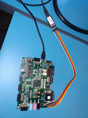
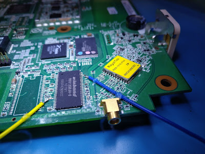
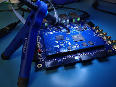
The target device chosen for testing was the NXP LPC1343, an ARM Cortex-M3 microcontroller. In order to control the input target voltage and coordinate glitches, the Digilent Arty A7 development board was used, built around the Xilinx Artix 7 FPGA. Custom gateware was developed for the Arty board, in order to facilitate control and triggering of glitches based on a variety of factors. For the purposes of this article, the two main triggers used are a GPIO line which goes high/low synchronized to certain device operations, and SWD signals corresponding to a “step” event. The source code for the FPGA gateware is available here.
In order to switch between the standard voltage level (Vdd) and the glitch voltage level (Vglitch), a Maxim MAX4617 Multiplexer IC was used. It is capable of switching between inputs in as little as 10ns, and is thus suitable for producing a glitch waveform on the LPC 1343 power rails with sufficient accuracy and timing.
As illustrated in the image above, the Arty A7 monitors a “trigger” line, either a GPIO output from the target or the SWD lines between the target and the debugger, depending on the mode of operation. When the expected condition is met, the A7 will drive the “glitch out” according to a provided waveform specifier, triggering a switch between Vdd and Vglitch via the Power Mux Circuit and feeding that to the target Vcore voltage line. A Segger J-Link was used to provide debug access to the target, and the SWD lines are also fed to the A7 for triggering.
In order to facilitate triggering on arbitrary SWD commands, a barebones SWD receiver was implemented on the A7. The receiver parses SWD transactions sniffed from the bus, and outputs the deserialized header and transaction data, values which can then be compared with a pre-configured target value. This allows for triggering of the glitchOut line based on any SWD data – for example, the S TEP and RESUME transactions, providing a means of timing glitches for single-stepped instructions.
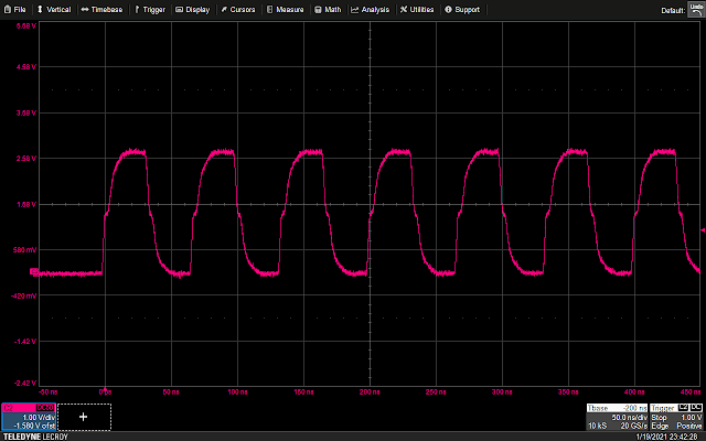
Prior to any direct testing of glitches performed while single-stepping instructions, observing glitches during normal operation and the effects they cause is helpful to provide a base understanding, as well as to provide a platform for making assumptions which can be tested later on. To provide an environment for observing the results of glitches of varied form and duration, program execution consists of a simple loop, incrementing and decrementing two variables. At each iteration, the value of each variable is checked against a known target value, and execution will break out of the loop when either one of the conditions is met. Outside of the loop, the values are checked against expected values and those values are transmitted via UART to the attacking PC if they differ.
Binary Ninja reverse engineering software was used to provide a visual representation of the compiled C. Because the assembly presented represents the machine code produced after compiling and linking, we can be sure that it matches the behavior of the processor exactly (ignoring concepts like parallel execution, pipelining etc. for now), and lean on that information when making assumptions about timing and processor behavior with regard to injecting faults.
Though simple, this environment provides a number of interesting targets for fault injection. Contained in the loop are memory access instructions (LDR, STR), arithmetic operations (ADDS, SUBS), comparisons, and branching operations. Additionally, the pulse of PIO2_6 provides a trigger for the glitchOut signal from the FPGA – depending on the delay applied to that signal, different areas/instructions in the overall loop may be targeted. By tracing the power consumption of the ARM core with a shunt resistor and transmission line probe, execution can be visualized.
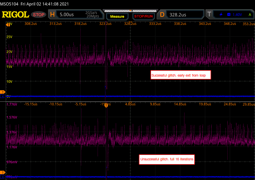
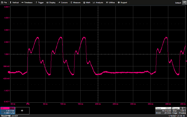
The following waveform shows the GPIO trigger line (blue), and the power trace coming from the LPC (purple). The GPIO line goes high for one cycle then low, signaling the start of the loop. What follows is a pattern which repeats 16 times, representing the 16 iterations of the loop. This is bounded on either side by the power trace corresponding to the code responsible for writing data to the UART, and branching back to the start of the main loop, which is fairly uniform.
We now have:
A reference of the actual instructions being executed by the processor (the disassembly via Binary Ninja)
A visual representation of that execution, viewable in real time as the processor executes (via the power trace)
A means of taking action within the system under test which can be calibrated based on the behavior of the processor (the FPGA glitcher).
Using the above information, it is possible to vary the offset of the glitch from the trigger, and (roughly) correlate that timing to a given instruction or group of instructions being executed. For example, by triggering a glitch sometime during the sixth repetition of the pattern on the power trace, we can observe that that portion of the power trace appears to be cut off early, and the values reported over UART by the target reflect some kind of misbehavior or corruption during the sixth iteration of the loop.
So far, the methodology employed has been in line with traditional fault injection parameter search techniques – optimize for visibility into a system to determine the most effective timing and glitch duration using some behavior baked into device operation (here, a GPIO line pulsing). While this provides coarse insight into the effects of a successfully injected fault (for the above example we can make the assumption that an operation at some point during the sixth iteration of the loop was altered, any more specificity is just speculation), it may have been a skipped load instruction, a corrupted store, or a flipped compare among many other possibilities.
To illustrate this point, the following is the parsed, sorted, and counted output of the UART traffic from the target device, after running the glitch for a few thousand iterations of the outer loop. The glitch delay and duration remained constant, but resulted in a fairly wide spread of discreet effects on the state of the variables at the end of the loop. Some entries are easy to reason about, such as the first and most common result: B is the expected value after six iterations (16 – 6 = 10), but A is 16, and thus a skipped LDR or STR instruction may have left the value 16 in the register placed there by previous operations. However, other results are harder to reason about, such as the entries containing ascii text, or entries where the variable with the incorrect value doesn’t appear to correlate to the iteration number of the loop.
This level of vagueness is acceptable in some applications of fault injection, such as breaking out of an infinite loop as is sometimes seen in secure boot bypass techniques. However, for more complex attacks where a particular operation needs to be corrupted in just the right way greater specificity, and thus a more granular understanding, is a necessity.
And so what follows is the novel portion of the research conducted for this article: creating a methodology for targeting fault injection attacks to single instructions, leveraging debug interfaces such as SWD/JTAG for instruction isolation and timing. In addition to the research value offered by this work, the developed methodology may also have practical applications under certain, not uncommon circumstances regarding devices in the wild as well, which will be discussed in a later section.
The Arm SWD interface uses a single bidirectional data connection and a separate clock to transfer data synchronously. An operation on the wire consists of two or three phases: packet request, acknowledgement response, and data transfer.
Of course, there’s more to it than that, but for the purposes of this article all we’re really interested in is the data transfer, thanks to a quirk of Cortex-M3 debugging registers: halting, stepping, and continuing execution are all managed by writes to the Debug Halting Control and Status Register (DHCSR). Additionally, writes to this register are always prefixed with 0xA05F, and only the low 4 bits are used to control the debug state — [MASKINTS, STEP, HALT, DEBUGEN] from high to low. So we can track STEP and RESUME actions by looking for SWD write transaction with the data 0xA05F0001 (RESUME) and 0xA05F000D (STEP).
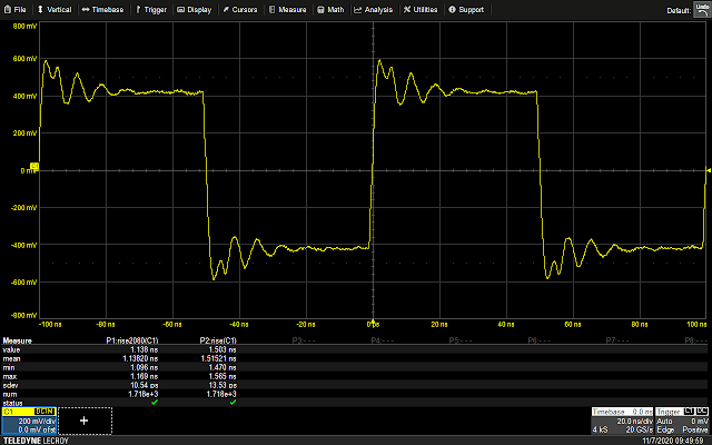
Because of the aforementioned bidirectionality of the protocol, it isn’t as easy as just matching a bit pattern: based on whether a read or write transaction is taking place, and which phase is currently underway, data may be valid on either clock edge. Beyond that, there are also turnaround periods that may or may not be inserted between phases, depending on the transaction. The simplest solution turned out to be just implementing half of the protocol, and discarding the irrelevant portions keeping only the data for comparison. The following is a Vivado ILA trace of the-little-SWD-implementation-that-could successfully parsing the STEP transaction sniffed from the SWD lines.
Isolating Instructions
So, by single stepping an instruction and sniffing the SWD lines from the A7, it is possible to trigger a glitch the instant (or very close to, within 10ns) the data is latched by the target board’s debug machinery. Importantly, because the target requires a few trailing SWCLK cycles to complete whatever actions the debug probe requires of it, there is plenty of wiggle room between the data being latched and the actual execution of the instruction. And indeed, thanks to the power trace, there is a clear indication of the start of processor activity after the SWD transaction completes.
As can be seen above, there is a delay of somewhere in the neighborhood of 4us, an eternity at the 100MHz of the A7. By delaying the glitch to various offsets into the “bump” corresponding to instruction execution, we can finally do what we came here to do: glitch a single-stepping processor.
In order to produce a result more interesting than “look, it works!” a simple script was written to manage the behavior of the debugger/processor via OpenOCD. The script has two modes: a “fast” mode, which single steps as fast as the debugger can keep up with used for finding the correct timing and waveform for glitches, and a (painfully) “slow” mode, which inspects registers and the stack before and after each glitch event, highlighting any unexpected behavior for perusal. Almost immediately, we can see some interesting results glitching a load register instruction in the middle of the innermost loop — in this case a LDR r3, [sp] which loads the previous value of the A variable into r3, to be incremented in the next instruction.
We can see that nothing has changed, suggesting that the operations simply didn’t occur or finish — a skipped instruction. This reliably leads to an off-by-one discrepancy in the UART output from the device: either A/B ends up 1 less/greater than it should be at the end of the loop, because one of the inc/dec operations was acting on data which is not actually associated with the state of the A variable.
Interestingly, this research shows that the effectiveness of fault injection is not limited only to instructions which access memory (LDR, STR, etc.), but can also be used to affect the execution of arithmetic operations, such as ADDS and CMP, or even branch instructions (though whether the instructions themselves are being corrupted or if the corruption is occurring on the ASPR by which branches are decided requires further study). In fact, no instruction tested for this article proved impervious to single-step-glitching, though the rate of success did vary depending on the instruction.
We see here the CMP instruction which determines whether or not A matches the expected 0x10 being targeted. We see that the xPSR is not updated (meaning the zero flag is not set and as far as the processor is concerned, the CMP’d values did not match, and so the values of A and B are sent via UART. However, because it was the CMP instruction itself being glitched, the reported values are the correct 0x10 and 0. Interestingly, we see that r1 has been updated to 0x10, the same immediate value used in the original CMP. Referring to the ARMv7 Architecture Reference Manual, the machine code for CMP r3, 0x10 should be 0x102b. Considering possible explanations for the observed behavior, one might consider an instruction like LDR or MOVS, which could have moved the value into the r1 register. And as it turns out, the machine code for MOVS r1, 0x10 is 0x1021, not too many bits away from the original 0x102b!
While that isn’t the definitive answer as to cause for the observed behavior, its a guess well beyond the level of information available via power trace analysis and similar techniques alone. And if it is correct, we not only know what generally occurred to cause this behavior, but can even see which bits specifically in the instruction were flipped for a given glitch delay/duration.
Including all the script output for every instruction type in this article is a bit impractical, but for the curious the logs detailing registers/stack before and after each successful glitch for each instruction type will be made available in the git repo hosting the glitcher code.
Practical Applications
I know what you’re thinking.
“If you have access to a device via JTAG/SWD debugger, why fuss with all the fault injection stuff? You can make the device do anything you want! In fact, I recently read a great blog postwhere I learned how to take advantage of an open JTAG interface!”
However, there is a very common configuration for embedded devices in the wild to which the research presented here could prove useful. Many devices, including the STM32 series (such as the DUT for this article), implement a sort of “high but not the highest possible” security mode, which allows for limited debugging capabilities, but prevents reads and writes to certain areas of memory, rendering the bulk of techniques for leveraging an open JTAG connection ineffective. This is chosen over the more secure option of disabling debugging entirely because the latter leaves no option for fixing or updating device firmware (without a custom bootloader), and many OEMs may choose to err towards serviceability rather than security. In most such implementations though, single stepping is still permitted!
In such a scenario, aided by a copy of device firmware, a probing setup analogous the one described here, or both, it may be possible to render an otherwise time-consuming and tedious attack nearly trivial, stripping away all the calibration and timing parameterization normally required for fault injection attacks. Need to bypass secure boot on a partially locked down device? No problem, just break on the CMP that checks the return value of is_secureboot_enabled().
Future Research
Further research is required to really categorize the applicability of this methodology during live testing, but the initial results do seems promising. Further testing will likely be performed on more realistic/practical device firmware, such as the previously mentioned secure boot scenario.
Additionally and more immediately, part two of this series of blog posts will continue to focus on developing a better understanding of what happens within an integrated circuit, and in particular a complex IC such as a CPU, when subjected to fault injection attacks. I have been putting together an 8-bit CPU out of 74 series discreet components in my spare time over the last few months and once complete it will make the perfect target for this research: the clock is controllable/steppable externally, and each individual module (the bus, ALU, registers, etc.) are accessible by standard oscilloscope probes and other equipment.
This should allow for incredibly close examination of system state under a variety of conditions, and make transitory issues caused by faults which are otherwise difficult to observe (for example an injected fault interfering with the input lines of the ALU but not the actual input registers) quite clear to see.
Stay tuned!
Video Demonstration
References
[1] J. Gratchoff, “Proving the wild jungle jump,” University of Amsterdam, Jul. 2015 [2] Y. Lu, “Injecting Software Vulnerabilities with Voltage Glitching,” Feb. 2019 [3] D. Nedospasov, “NXP LPC1343 Bootloader Bypass,” Aug. 2017, https://toothless.co/blog/bootloader-bypass-part1/ [4] C. Gerlinsky, “Breaking Code Read Protection on the NXP LPC-family Microcontrollers,” Jan. 2017, https://recon.cx/2017/brussels/talks/breaking_crp_on_nxp.html [5] A. Barenghi, G. Bertoni, E. Parrinello, G. Pelosi, “Low Voltage Fault Attacks on the RSA Cryptosystem,” 2009
ADVISORIES | March 2, 2021
CNJ PJeOffice Remote Code Execution in Update Mechanism
By
Tiago Assumpcao
& Robert Connolly
Brasil CNJ’s Processo Judicial Eletrônico (PJe) system processes judicial data with the objective of fulfilling the needs of the Brazilian Judiciary Power: the Superior, Military, Labor, and Electoral Courts; the courts of both the Federal Union and individual states; and specialized justice systems that handle ordinary law and employment tribunals at both the federal and state level.
The main goal of PJeOffice is to guarantee the legal authenticity and integrity of documents and processes through digital signatures. It is employed by lawyers, judges, and high-level officials, such as prosecutors and ministers.
The application’s update system is vulnerable to remote code execution, with two immediate implications.
A Practical Approach to Attacking IoT Embedded Designs (II)
By
Ruben Santamarta
In this second and final blog post on this topic, we cover some OTA vulnerabilities we identified in wireless communication protocols, primarily Zigbee and BLE.
As in the previous post, the findings described herein are intended to illustrate the type of vulnerabilities a malicious actor could leverage to attack a specified target to achieve DoS, information leakage, or arbitrary code execution.
These vulnerabilities affect numerous devices within the IoT ecosystem. IOActive worked with the semiconductor vendors to coordinate the disclosure of these security flaws, but it is worth mentioning that due the specific nature of the IoT market and despite the fact that patches are available, a significant number of vulnerable devices will likely never be patched.
As usual, IOActive followed a responsible disclosure process, notifying the affected vendors and coordinating with them to determine the proper time to disclose issues. In general terms, most vendors properly handled the disclosure process.
At the time of publishing this blog post, the latest versions of the affected SDKs contain fixes for the vulnerabilities. Please note that IOActive has not verified these patches.
OTA Vulnerabilities
Affected vendors
Nordic Semiconductor
Texas Instruments
Espressif Systems
Qualcomm
Nordic Semiconductor – www.nordicsemi.com
Vulnerability
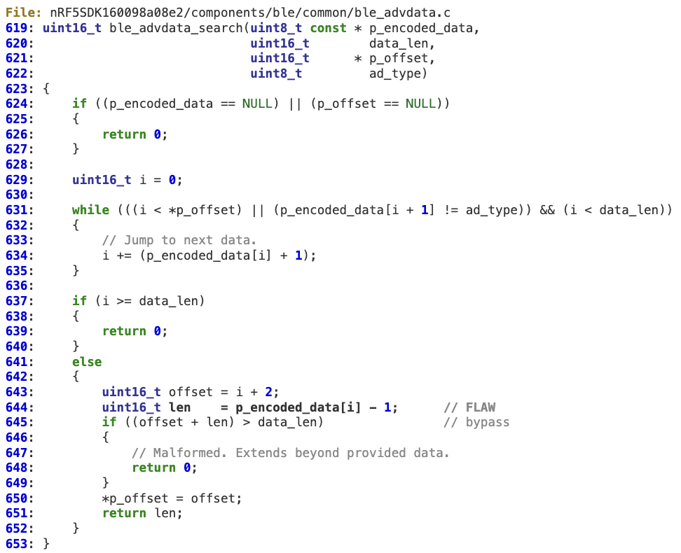
Integer overflow in ‘ble_advdata_search’
Affected Products
nRF5 SDK prior to version 16
Background
“The nRF5 SDK is your first stop for building fully featured, reliable and secure applications with the nRF52 and nRF51 Series. It offers developers a wealth of varied modules and examples right across the spectrum including numerous Bluetooth Low Energy profiles, Device Firmware Upgrade (DFU), GATT serializer and driver support for all peripherals on all nRF5 Series devices. The nRF5 SDK will almost certainly have something for your needs in developing exciting yet robust wireless products” https://www.nordicsemi.com/Software-and-tools/Software/nRF5-SDK
Impact
A malicious actor able to send specially crafted BLE advertisements could leverage this vulnerability to execute arbitrary code in the context of a device running a nRF5-SDK-based application. This may lead to the total compromise of the affected device.
Technical Details
At line 644, an attacker-controlled buffer pointed to by ‘p_encoded_data[i]’ may be 0x00, which will overflow ‘len’, whose value will be 0xFFFF after the operation.
This effectively bypasses the sanity check at line 645.
Exploitation
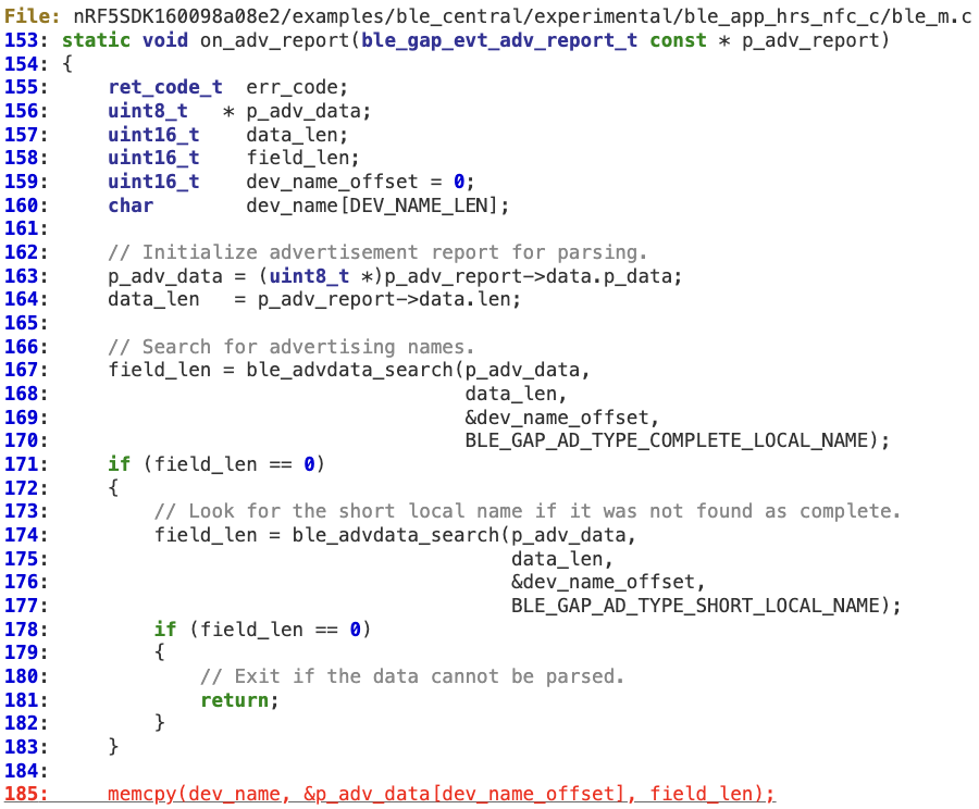
Different scenarios are possible depending on how ‘len’ is handled by the caller. In the following example, this vulnerability leads to a classic stack overflow at line 185.
Vulnerability
Incorrect DFU packet length resulting in remote code execution
A malicious actor able to initiate a DFU connection to the affected device could potentially leverage this vulnerability to execute arbitrary code in the context of the bootloader. This may lead to the total compromise of the affected device.
Technical Details
When the bootloader handles DFU messages, the length of the mesh advertising data packets is not properly checked. The vulnerable code path is as follows:
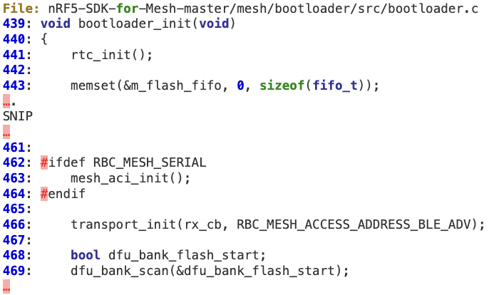
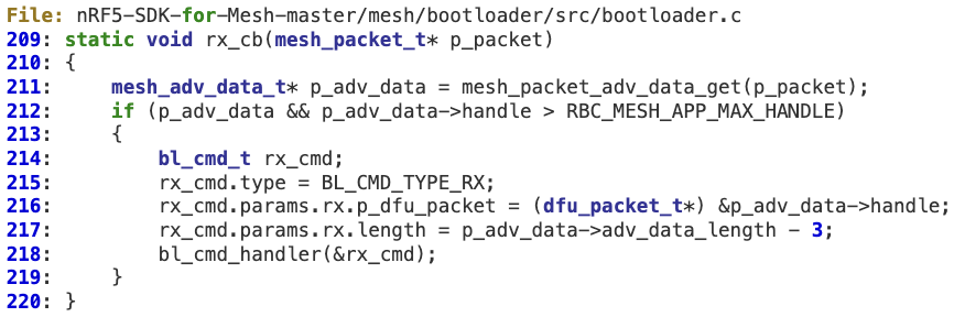
1. In ‘bootloader_init’ at line 466, the rx callback is initialized to ‘rx_cb’ by ‘transport_init’.
2. At line 211, the advertising packet queue is checked for DFU packets by calling ‘mesh_packet_adv_data_get’, which does not perform proper validation of the ‘adv_data_length’ field (e.g. by checking for a minimum value [ > 3 ]). As a result at line 217, ‘p_adv_data->adv_data_length‘ (8-bit) may wrap to a large 32-bit value, which is stored at ‘rx_cmd.params.rx.length’.
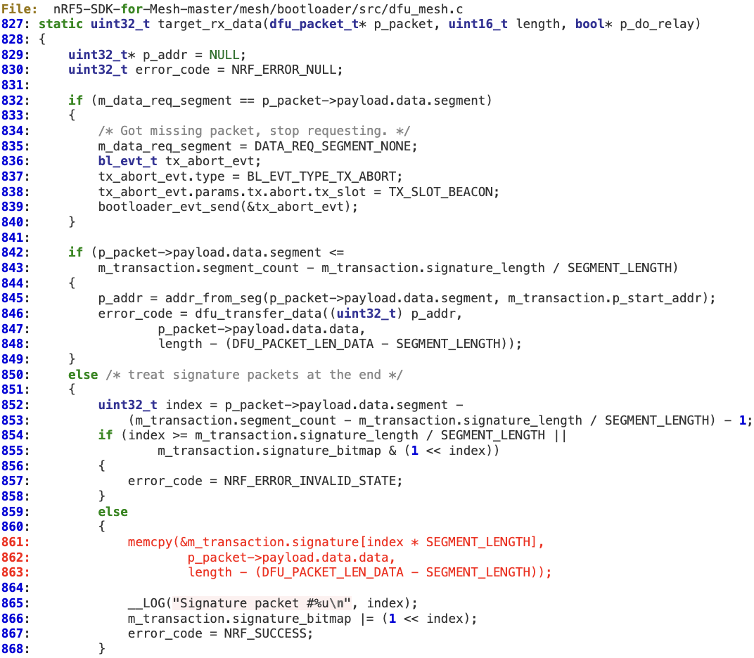
3. A ‘signature’ packet is then routed, without checking the length (truncated to 16-bit at ‘bl_cmd_handler’), through ‘bl_cmd_handler’-> ‘dfu_mesh_rx’ -> ‘handle_data_packet’ and finally ‘target_rx_data’, where the memory corruption may occur at line 861.
Vulnerability
Multiple buffer overflows when handling Advertising Bearer data packets
Affected Products
nRF5 SDK for Mesh prior to version 4.1.0
Background
“The nRF5 SDK is your first stop for building fully featured, reliable and secure applications with the nRF52 and nRF51 Series. It offers developers a wealth of varied modules and examples right across the spectrum including numerous Bluetooth Low Energy profiles, Device Firmware Upgrade (DFU), GATT serializer and driver support for all peripherals on all nRF5 Series devices. The nRF5 SDK will almost certainly have something for your needs in developing exciting yet robust wireless products” https://www.nordicsemi.com/Software-and-tools/Software/nRF5-SDK
Impact
A malicious actor able to send malicious Advertising Bearer packets to the affected device could potentially leverage this vulnerability to execute arbitrary code. This may lead to the total compromise of the affected device.
Technical Details
The length of the Advertising Bearer data packets is not properly checked. The vulnerable code path is as follows:
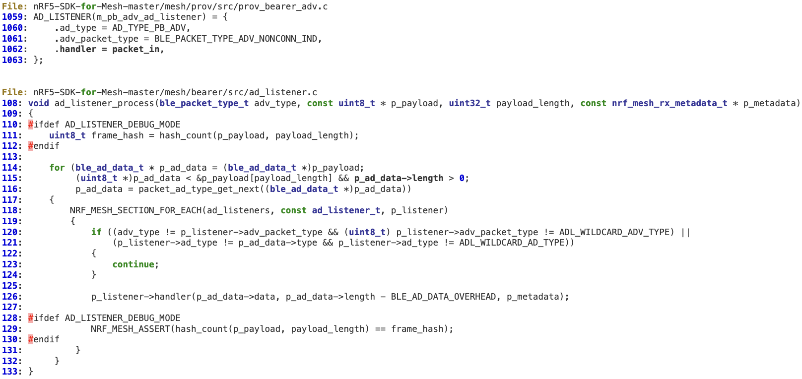
1. When an AD listener is dispatched (it has been previously registered at line 1062 in ‘prov_bearer_adv.c‘), there is just one action performed to sanitize the length, at line 115 ( > 0 ).
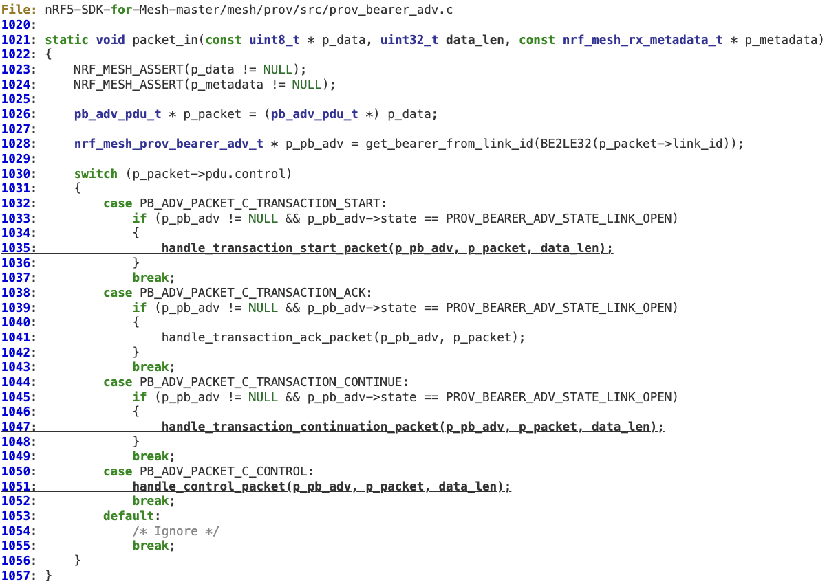
2. The handler for Advertising Bearer packets does not perform any additional validation on the received ‘length’, which is then propagated to specific packet handling functions at lines 1035, 1047, and 1051.
3. ‘handle_transaction_start_packet’ does not perform any validation on ‘length’ before reaching lines 706 (underflow) and 707 (buffer overflow).
4. ‘handle_transaction_continuation_packet’ does not perform any validation on ‘length’ before reaching lines 759 (underflow) and 760 (buffer overflow).
Vulnerability
Buffer overflow in BLE Queued Writes
Affected Products
nRF5 SDK prior to version 16
Background
“The nRF5 SDK is your first stop for building fully featured, reliable and secure applications with the nRF52 and nRF51 Series. It offers developers a wealth of varied modules and examples right across the spectrum including numerous Bluetooth Low Energy profiles, Device Firmware Upgrade (DFU), GATT serializer and driver support for all peripherals on all nRF5 Series devices. The nRF5 SDK will almost certainly have something for your needs in developing exciting yet robust wireless products” https://www.nordicsemi.com/Software-and-tools/Software/nRF5-SDK
Impact
A malicious actor able to send a initiate a Queued Write request to the affected device could potentially leverage this vulnerability to execute arbitrary code. This may lead to the total compromise of the affected device.
Technical Details
‘val_offset’ and ‘val_len’ are not properly sanitized. As a result, a malicious request containing a specific combination of both values (containing a large ‘val_len’ value) may lead to an integer overflow at line 135, resulting in a value that can bypass the check at line 136. Finally, at line 138, the overflow occurs as ‘val_len’ is used in the memcpy operation.
Texas Instruments – www.ti.com
Vulnerability
Z-Stack – Multiple heap overflows in ZCL parsing functions
Affected Products
SIMPLELINK-CC13X2-26X2-SDK prior to version 4.40.00.44 Other Zigbee stacks based on the Z-Stack code are also affected (i.e. Telink)
“Z-Stack is a component of the SimpleLink™ CC13x2 / CC26x2 Software Development Kit. This component enables development of Zigbee® 3.0 specification based products. Z-Stack is TI’s complete solution for developing certified Zigbee 3.0 solution on CC13x2 and CC26x2 platforms. Z-Stack contained in this release is based on Zigbee 3.0 specification with the added benefit of running on top of TI-RTOS.” https://www.ti.com/tool/Z-STACK
Impact
A malicious actor in possession of the NWK key (authenticated to the Zigbee Network) may send OTA malicious Zigbee ZCL packets to the victim’s node, which may result in the execution of arbitrary code in the context of the affected device.
Technical Details
Z-Stack parses the ZCL payloads by performing a two-steps flawed logic:
1. It calculates the total length of the attributes by iterating over the incoming ZCL frame payload without checking for integer overflows.
2. Dynamic memory is allocated according to this total length; however, attributes are individually copied to the parsing structure without sanitizing its length.
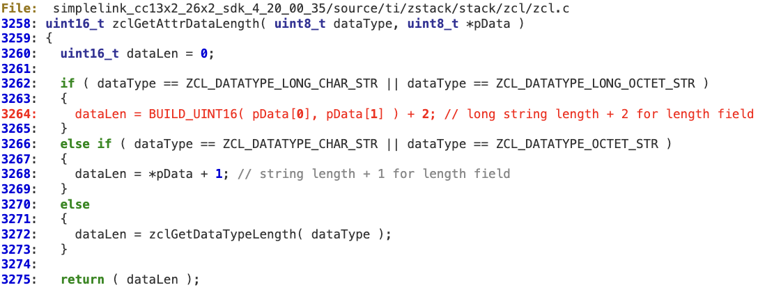
In the following example, the first step can be mapped to the ‘while’ loop at lines 3699-3718.
‘dataLen’ is intended to hold the total length of the attributes in the message. Each length is individually calculated in ‘zclGetAttrDataLength’.
There is neither an overflow check for ‘dataLen’ nor a bounds check in the last iteration of the loop against ‘pBuf’ before adding the value to ‘dataLen’. According to this logic, an attacker can create a ZCL payload containing a specific combination of attributes that may force the ‘dataLen’ integer to be wrapped, holding a value lower than the actual total length.
Attribute 1: type: long octet string: length : 0x6 (+2) Attribute 2: type: long octet string: length: 0x10 (+2) Attribute 3: type: long octet string: length: 0xFFF0 (+2) Total length (truncated to 16-bit as in ‘dataLen’) = 0xC
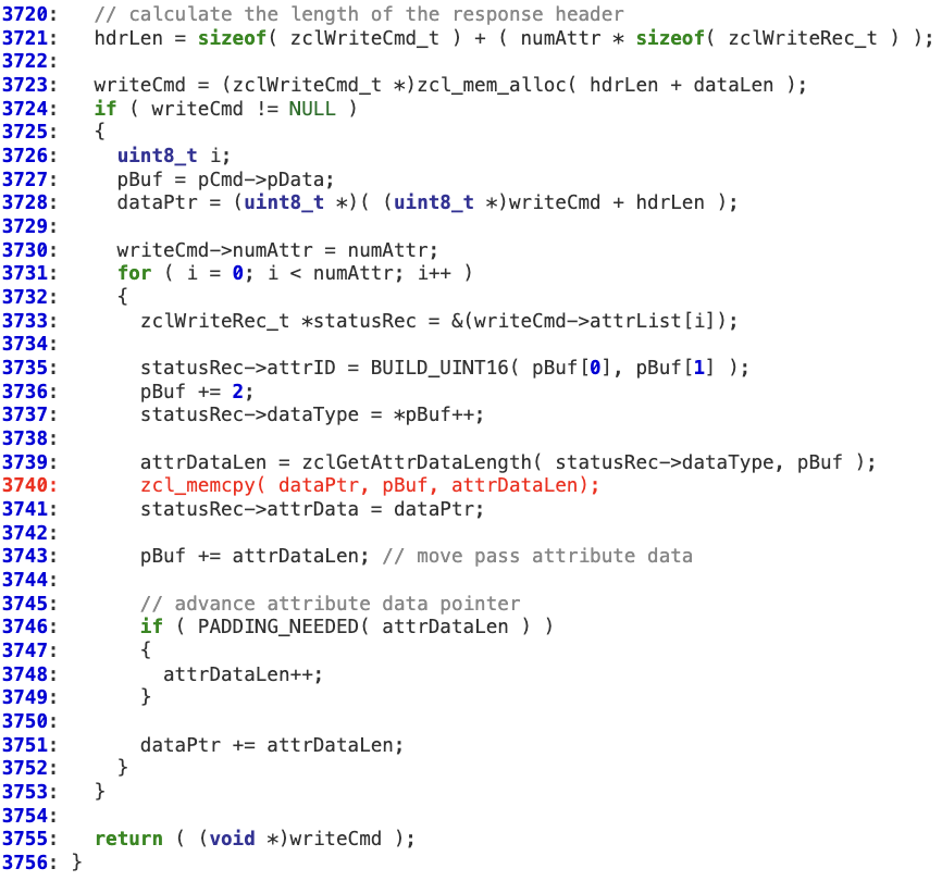
Back in ‘zclParseInWriteCmd’, ‘dataLen’ is used to allocate the buffer where the attributes’ data will be copied. As there is no sanity check on the consistency of this memory allocation (line 3723 is allocating less memory than expected due to the ‘dataLen’ overflow), this operation may result in a memory corruption at line 3740 (memcpy) as ‘attrDataLen’ may be higher than the buffer allocated at ‘dataPtr’.
Most of the parsing routines in ‘zclCmdTable’ are affected.
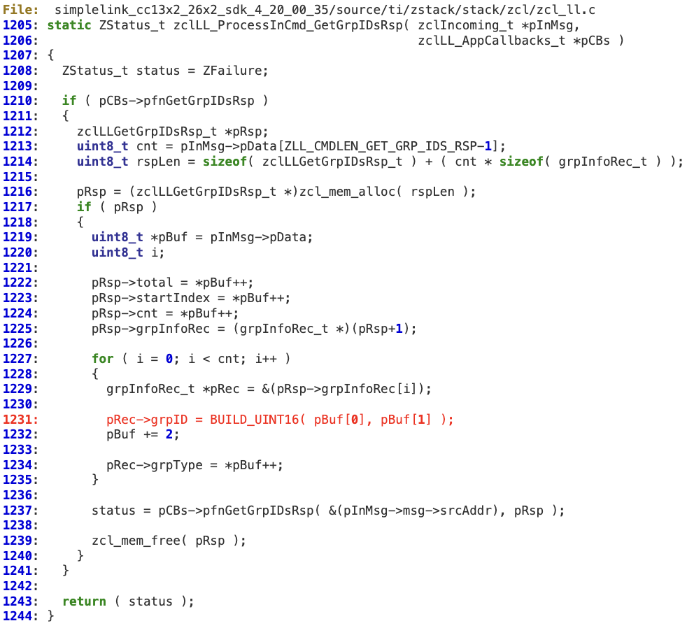
Additionally, there is an integer overflow in the way ‘zclLL_ProcessInCmd_GetGrpIDsRsp’ (also ‘zclLL_ProcessInCmd_GetEPListRsp’ and ‘zclLL_ProcessInCmd_DeviceInfoRsp’) parses the incoming message, as ‘cnt’ is not properly sanitized before allocating the buffer (line 1214). As a result, ‘rspLen’ wraps around, holding a value which is actually lower than ‘cnt’. Later on ‘cnt’ is used as the test expression in the ‘for’ loop (lines 1227) so it will end up triggering memory corruption at line 1231.
Vulnerability
EasyLink – memory corruption in ‘rxDoneCallback’
Affected Products
SIMPLELINK-CC13X2-26X2-SDK prior to version 4.40.00.44
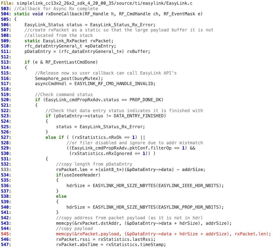
A remote attacker may send a specially crafted OTA EasyLink packet to the victim’s device, which may result in either a DoS condition or the execution of arbitrary code.
Technical Details
EasyLink does not properly validate the length of the received packet. At line 533, the attacker-controlled buffer (‘pDataEntry->data‘) is used to extract 1 byte that is then used to calculate the number of bytes that will be copied (at line 545) to the static buffer pointed to by ‘rxBuffer.payload‘ (fixed at 128 bytes).
Espressif Systems – www.espressif.com
Vulnerability
Protocomm ‘transport_simple_ble_read’ information leak
“Espressif provides basic hardware and software resources to help application developers realize their ideas using the ESP32 series hardware. The software development framework by Espressif is intended for development of Internet-of-Things (IoT) applications with Wi-Fi, Bluetooth, power management and several other system features.” https://docs.espressif.com/projects/esp-idf/en/latest/esp32/get-started/
This bug was awarded a $2,229 bounty as part of the ESP32 bug bounty program (https://www.espressif.com/en/news/bug-bounty), which was donated by Espressif, on my behalf, to a Spanish animal rescue organization.
Impact
A remote attacker may send a specially crafted BLE packet to the victim’s device, which may result in either a DoS condition or an information leak.
Technical Details
When handling a BLE READ request from the client, ‘offset’ is not properly sanitized before copying data to the response (line 128). As a result, a malicious client may leak sensitive information from the device by setting an overly large ‘offset’ parameter in the READ request.
Qualcomm – www.qualcomm.com
Vulnerability
‘Api_ParseInfoElem’ improper handling of IEEE80211_ELEMID_RSN length may lead to a remote DoS
Affected Products
Qualcomm WIFI_QCA Middleware
Background
“The QCA4004 is an intelligent platform for the Internet of Things that contains a low-power Wi-Fi connectivity solution on a single chip. It includes a number of TCP/IP-based connectivity protocols along with SSL, allowing a low-cost, low-complexity system to obtain full-featured internet connectivity and reliable information exchange.” https://www.qualcomm.com/products
Impact
A malicious actor able to send malicious 802.11 management frames to the affected device may potentially leverage this vulnerability to perform a DoS, as unmapped or invalid memory may be hit when parsing RSN IEs after a SCAN operation has been invoked.
Technical Details
The vulnerable code path is as follows:
1. When parsing the RSN IE, its length (‘ie_len’) is not properly sanitized against ‘len’ before calling ‘security_ie_parse’.
‘security_ie_parse’ does not perform any additional validation on the received ‘ie_len’. Then ‘ie_len’ is decremented at 637, 644, and 658 without performing any check for alignment or underflow, so a specific value in ‘ie_len’ makes the second condition in the ‘for’ loop (line 647) always true.
As a result, this ‘for’ loop only depends on the first condition (where ‘cnt’ is also controlled by the potential attacker). This situation may force the ‘for’ loop to run beyond the original buffer’s bound, potentially hitting unmapped or invalid memory.
INSIGHTS, RESEARCH |
Probing and Signal Integrity Fundamentals for the Hardware Hacker, part 2: Transmission Lines, Impedance, and Stubs
By
Andrew Zonenberg
This is the second post in our ongoing series on the troubles posed by high-speed signals in the hardware security lab.
What is a High-speed Signal?
Let’s start by defining “high-speed” a bit more formally:
A signal traveling through a conductor is high-speed if transmission line effects are non-negligible.
That’s nice, but what is a transmission line? In simple terms:
A transmission line is a wire of sufficient length that there is nontrivial delay between signal changes from one end of the cable to the other.
You may also see this referred to as the wire being “electrically long.”
Exactly how long this is depends on how fast your signal is changing. If your signal takes half a second (500ms) to ramp from 0V to 1V, a 2 ns delay from one end of a wire to the other will be imperceptible. If your rise time is 1 ns, on the other hand, the same delay is quite significant – a nanosecond after the signal reaches its final value at the input, the output will be just starting to rise!
Using the classical “water analogy” of circuit theory, the pipe from the handle on your kitchen sink to the spout is probably not a transmission line – open the valve and water comes out pretty much instantly. A long garden hose, on the other hand, definitely is.
Propagation Delay
The exact velocity of propagation depends on the particular cable or PCB geometry, but it’s usually somewhere around two thirds the speed of light or six inches per nanosecond. You may see this specified in cable datasheets as “velocity factor.” A velocity factor of 0.6 means a propagation velocity of 0.6 times the speed of light.
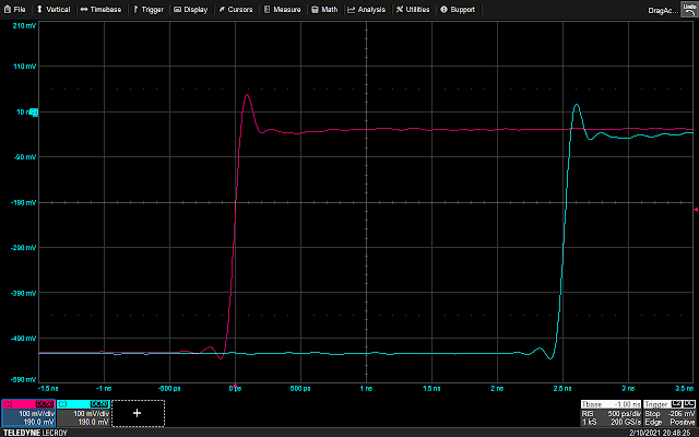
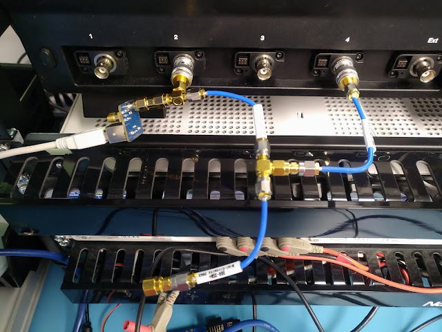
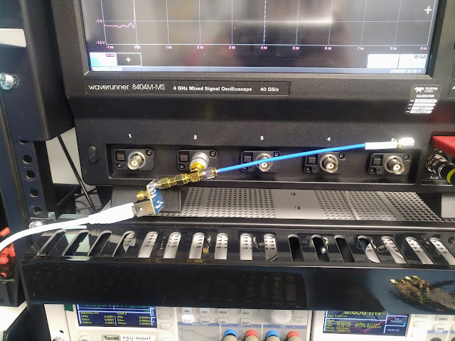
Let’s make this a bit more concrete by running an experiment: a fast rising edge from a signal generator is connected to a splitter (the gray box in the photo below) with one output fed through a 3-inch cable to an oscilloscope input, and the other through a much longer 24-inch cable to another scope input.
Experimental setup for propagation delay demonstration
This is a 21-inch difference in length. The cable I used for this test (Mini-Circuits 086 series Hand-Flex) uses PTFE dielectric and has a velocity factor of about 0.695. Plugging these numbers into Wolfram Alpha, we get an expected skew of 2.56 ns:
Calculating expected propagation delay for the experiment
Sure enough, when we set the scope to trigger on the signal coming off the short cable, we see the signal from the longer cable arrives a touch over 2.5 ns later. The math checks out!
Experimental observation of cable delay
As a general rule for digital signals, if the expected propagation delay of your cable or PCB trace is more than 1/10 the rise time of the signal in question, it should be treated as a transmission line.
Note that the baud rate/clock frequency is unimportant! In the experimental setup above, the test signal has a frequency of only 10 MHz (100 ns period) but since the edges are very fast, cable delay is easily visible and thus it should be treated as a transmission line.
This is a common pitfall with modern electronics. It’s easy to look at a data bus clocked at a few MHz and think “Oh, it’s not that fast.” But if the I/O pins on the device under test (DUT) have sharp edges, as is typical for modern parts capable of high data rates, transmission line effects may still be important to consider.
Impedance, Reflections, and Termination
If you open an electrical engineering textbook and look for the definition of impedance you’re probably going to see pages of math talking about cable capacitance and inductance, complex numbers, and other mumbo-jumbo. The good news is, the basic concept isn’t that difficult to understand.
Imagine applying a voltage to one end of an infinitely long cable. Some amount of current will flow and a rising edge will begin to travel down the line. Since our hypothetical cable never ends, the system never reaches a steady state and this current will keep flowing at a constant level forever. We can then plug this voltage and current into Ohm’s law (V=I * R) and solve for R. The transmission line thus acts as a resistor!
This resistance is known as the “characteristic impedance” of the transmission line, and depends on factors such as the distance from signal to ground, the shape of the conductors, and the dielectric constant of the material between them. Most coaxial cable and high-speed PCB traces are 50Ω impedance (because this is a round number, a convenient value for typical material properties at easily manufacturable dimensions, and more) although a few applications such as analog television use 75Ω and other values are used in some specialized applications. The remainder of this discussion assumes 50Ω impedance for all transmission lines unless otherwise stated.
What happens if the line forks? We have the same amount of current flowing in since the line has a 50Ω impedance at the upstream end, but at the split it sees 25Ω (two 50Ω loads in parallel). The signal thus reduces in amplitude downstream of the fork, but otherwise propagates unchanged.
There’s just one problem: at the point of the split, we have X volts in the upstream direction and X/2 volts in the downstream direction! This is obviously not a stable condition, and results in a second wavefront propagating back upstream down the cable. The end result is a mirrored (negative) copy of the incident signal reflecting back.
We can easily demonstrate this effect experimentally by placing a T fitting at the end of a cable and attaching additional cables to both legs of the fitting. The two cables coming off the T are then terminated (one at a scope input and the other with a screw-on terminator). We’ll get to why this is important in a bit.
Experimental setup for split in transmission line
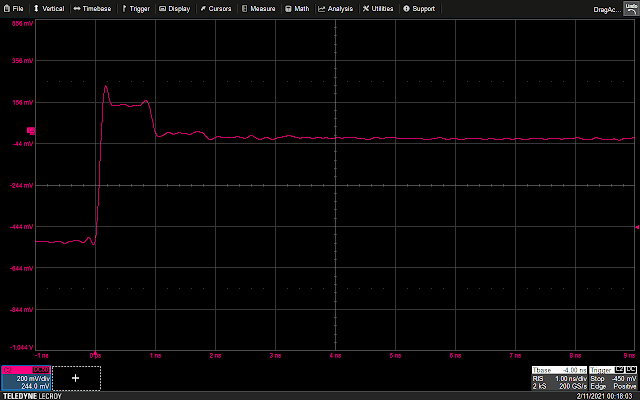
The cable from the scope input to the split is three inches long; using the same 0.695 velocity factor as before gives a propagation delay of 0.365 ns. So for the first 0.365 ns after the signal rises everything is the same as before. Once the edge hits the T the reduced-voltage signal starts propagating down the two legs of the T, but the same reduced voltage also reflects back upstream.
Observed waveform from split test
It takes another 0.365 ns for the reflection to reach the scope input so we’d expect to see the voltage dip at around 0.73 ns (plus a bit of additional delay in the T fitting itself) which lines up nicely with the observed waveform.
In addition to an actual T structure in the line, this same sort of negative reflection can be caused by any change to a single transmission line (different dielectric, larger wire diameter, signal closer to ground, etc.) which reduces the impedance of the line at some point.
Up to this point in our analysis, we’ve only considered infinitely long wires (and the experimental setups have been carefully designed to make this a good approximation). What if our line is somewhat long, but eventually ends in an open circuit? At the instant that the rising edge hits the end of the wire, current is flowing. It can’t stop instantaneously as the current from further down the line is still flowing – the source side of the line has no idea that anything has changed. So the edge goes the only place it can – reflecting down the line towards the source.
Our experimental setup for this is simple: a six-inch cable with the other end unconnected.
Experimental setup for open circuit at end of a transmission line
Using the same 0.695 velocity factor, we’d expect our signal to reach the end of the cable in about 0.73 ns and the reflection to hit the scope at 1.46 ns. This is indeed what we see.
Observed waveform from open circuit test
Sure enough, we see a reflected copy of the original edge. The difference is, since the open circuit is a higher-than-matched impedance instead of lower like in the previous experiment, the reflection has a positive sign and the signal amplitude increases rather than dropping.
A closer inspection shows that this pattern of reflections repeats, much weaker, starting at around 3.0 ns. This is caused by the reflection hitting the T fitting where the signal generator connects to the scope input. Since the parallel combination of the scope input and signal generator is not an exact 50Ω impedance, we get another reflection. The signal likely continues reflecting several more times before damping out completely, however these additional reflections are too small to show up with the current scope settings.
So if a cable ending in a low impedance results in a negative reflection, and a cable ending in a high impedance results in a positive reflection, what happens if the cable ends in an impedance equal to that of the cable – say, a 50Ω resistor? This results in a matched termination which suppresses any reflections: the incident signal simply hits the resistor and its energy is dissipated as heat. Terminating high-speed lines (via a resistor at the end, or any of several other possible methods) is critical to avoid reflections degrading the quality of the signal.
One other thing to be aware of is that the impedance of circuit may not be constant across frequency. If there is significant inductance or capacitance present, the impedance will have frequency-dependent characteristics. Many instrument inputs and probes will specify their equivalent resistance and capacitance separately, for example “1MΩ || 17 pF” so that the user can calculate the effective impedance at their frequency of interest.
Stub Effects and Probing
We can now finally understand why the classic reverse engineering technique of soldering long wires to a DUT and attaching them to a logic analyzer is ill-advised when working with high speed systems: doing so creates an unterminated “stub” in the transmission line.
Typical logic analyzer inputs have high input impedances in order to avoid loading down the signals on the DUT. For example, the Saleae Logic Pro 8 has an impedance of 1MΩ || 10 pF and the logic probe for the Teledyne LeCroy WaveRunner 8000-MS series oscilloscopes is 100 kΩ || 5 pF. Although the input capacitance does result in the impedance decreasing at higher frequencies, it remains well over 50Ω for the operating range of the probe.
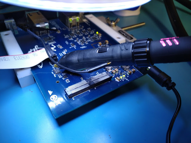
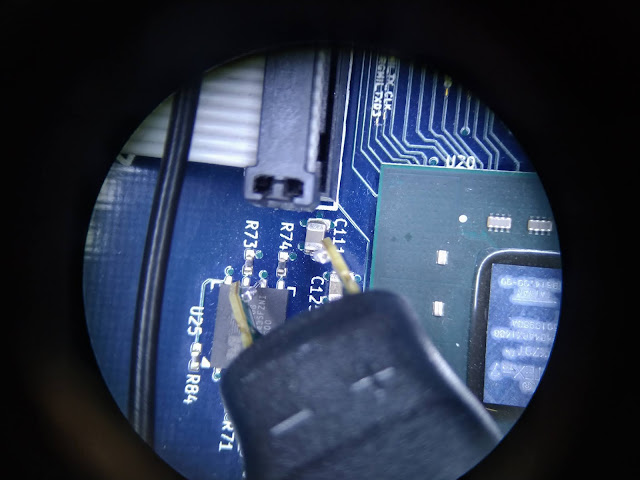
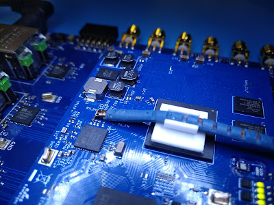
This means that if the wire between the DUT and the logic analyzer is electrically long, the signal will reflect off the analyzer’s input and degrade the signal as seen by the DUT. To see this in action, let’s do an experiment on a real board which boots from an external SPI flash clocked at a moderately fast speed – about 75 MHz.
As a control, we’ll first look at the signal using an electrically short probe. I’ll be using a Teledyne LeCroy D400A-AT, a 4 GHz active differential probe. This is a very high performance probe meant for non-intrusive measurements on much faster signals such as DDR3 RAM.
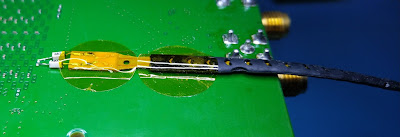
Active probe on SPI flash
Probe tip seen through microscope
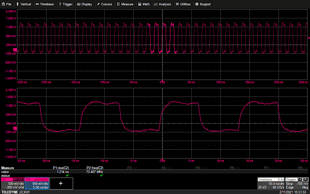
Looking at the scope display, we see a fairly clean square wave on the SPI SCK pin. There’s a small amount of noise and some rounding of the edges, but nothing that would be expected to cause boot failures.
Observed SPI SCK waveform
The measured SPI clock frequency is 73.4 MHz and the rise time is 1.2 ns. This means that any stub longer than 120 ps round trip (60 ps one way) will start to produce measurable effects. With a velocity of 0.695, this comes out to about half an inch. You may well get away with something a bit longer (“measurable effects” does not mean “guaranteed boot failure”), but at some point the degradation will be sufficient to cause issues.
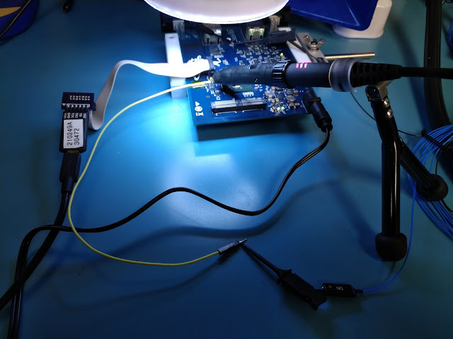
Now that we’ve got our control waveform, let’s build a probing setup more typical of what’s used in lower speed hardware reverse engineering work: a 12-inch wire from a common rainbow ribbon cable bundle, connected via a micro-grabber clip to a Teledyne LeCroy MSO-DLS-001 logic probe. The micro-grabber is about 2.5 inches in length, which when added to the wire comes to a total stub of about 14.5 inches.
(Note that the MSO-DLS-001 flying leads include a probe circuit at the tip, so the length of the flying lead itself does not count toward the stub length. When using lower end units such as the Saleae Logic that use ordinary wire leads, the logic analyzer’s lead length must be considered as part of the stub.)
Experimental setup with long probe stub wire (yellow)
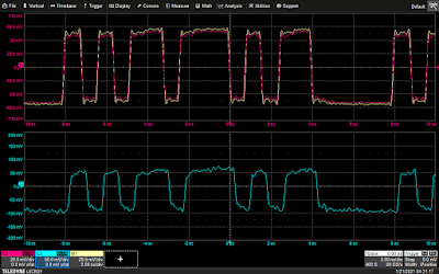
We’d thus expect to see a reflection at around 3.5 ns, although there’s a fair bit of error in this estimate because the velocity factor of the cable is unspecified since it’s not designed for high-speed use. We also expect the reflections to be a bit more “blurry” and less sharply defined than in the previous examples, since the rise time of our test signal is slower.
Measured SPI clock waveform with long stub wire
There’s a lot of data to unpack here so let’s go over it piece by piece.
First, we do indeed see the expected reflection. For about the first half of the cycle – close to the 3.5 ns we predicted – the waveform is at a reduced voltage, then it climbs to the final value for the rest of the cycle.
Second, there is significant skew between the waveform seen by the analog probe and the logic analyzer, which is caused by the large difference in length between the path from the DUT to the two probe inputs.
Third, this level of distortion is very likely to cause the DUT to malfunction. The two horizontal cursors are at 0.2 and 0.8 times the 1.8V supply voltage for the flash device, which are the logic low and high thresholds from the device datasheet. Any voltage between these cursors could be interpreted as either a low or a high, unpredictably, or even cause the input buffer to oscillate.
During the period in which the clock is supposed to be high, more than half the time is spent in this nondeterministic region. Worst case, if everything in this region is interpreted as a logic low, the clock will only appear to be high for about a quarter of the cycle! This would likely act like a glitch and result in failures.
Most of the low period is spent in the safe “logic low” range, however it appears to brush against the nondeterministic region briefly. If other noise is present in the DUT, this reflection could be interpreted as a logic high and also create a glitch.
Conclusions
As electronics continue to get faster, hardware hackers can no longer afford to remain ignorant of transmission line effects. A basic understanding of these physics can go a long way in predicting when a test setup is likely to cause problems.
INSIGHTS, RESEARCH | February 11, 2021
A Practical Approach To Attacking IoT Embedded Designs (I)
By
Ruben Santamarta
The booming IoT ecosystem has meant massive growth in the embedded systems market due to the high demand for connected devices. Nowadays, designing embedded devices is perhaps easier than ever thanks to the solutions, kits, chips, and code that semiconductor manufacturers provide to help developers cope with the vast number of heterogeneous requirements IoT devices should comply with.
This never-ending race to come up with new features within tight deadlines comes at a cost, which usually is paid in the security posture of the commercialized device.
Let’s assume a product vendor has implemented security best practices and everything has been locked down properly. Our goal is to compromise the device, but we don’t have access to any of the custom code developed for that specific device (not even in binary form). What about the code semiconductor vendors provide? How secure is the code in all those SDKs and middleware that IoT devices rely on?
I performed a manual code review of some of the most widely used IoT SDKs in order to try to answer this question and found multiple vulnerabilities in the code provided by leading semiconductor vendors, such as Texas Instruments, Nordic, and Qualcomm.
As usual, IOActive followed a responsible disclosure process, notifying the affected vendors and coordinating with them to determine the proper time to disclose issues. In general terms, most vendors properly handled the disclosure process.
At the time of publishing this blog post, the latest versions of the affected SDKs contain fixes for the vulnerabilities. Please note that IOActive has not verified these patches.
Introduction
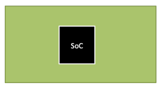
Embedded IoT systems need to be designed for specific functions. As a result, we can’t use a single reference design; however, it is possible to summarize the most common architectures.
SoC
These designs rely on an SoC that combines the MCU and communications transceiver into a single-chip solution. Thus, the wireless software stack and the application software run in the same component.
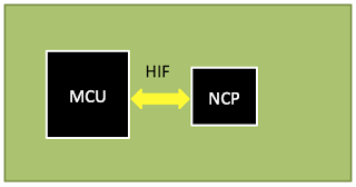
MCU + Transceiver
In these designs, the MCU is in charge of running the required software, including the applications and even part of the wireless stack, and the transceiver usually handles the physical and data link layers. In addition, there is a host interface (HIF), which is responsible for handling communication between the MCU (Host) and the transceiver, usually over a serial bus (e.g. SPI, UART, or I2C).
MCU + Network Co-Processor
These designs are a variant of the previous one, where the transceiver is swapped for a network co-processor (NCP), which runs the entire communications stack. In this architecture, the application is still running in the MCU (Host), while the network stack operations are entirely offloaded to the NCP. The HIF is still necessary to enable communication between the Host and NCP.
Attack Surface
As we have just outlined, the components within an embedded IoT design do not operate in isolation. They interact with the outside world via wireless and at the intra-board level with other chips.
1. Intra-board
Most current high-end MCUs and SoCs support some kind of secure boot or code integrity mechanism. Assuming a worst-case scenario (from an attacker’s perspective) where the vendor has closed the usual doors before deploying the product, we may face a pure black-box scenario, where we can’t dump or access the firmware.
In order to turn this situation to our favor, we can focus on the HIF code usually found in the SDKs from semiconductor vendors.
The advantage we have in this scenario is that, despite the fact that the firmware running in the Host MCU (Host from now on) may be unknown, analysis of HIF communications may reveal that the Host firmware has been compiled with potentially vulnerable SDK code.
A successful exploit targeting the HIF implementation could open the door to execute code in the Host if a local attacker has the ability to impersonate the transceiver/NCP over the HIF’s bus (SPI, UART, I2C, USB, etc.). At IOActive, we have been exploiting this attack vector for years in order to compromise among other devices, smart meters, which usually implement either an ‘MCU + NCP’ or ‘MCU + Transceiver’ design.
The vulnerabilities described in this post are intended to illustrate common patterns in the HIF layer implementation across different vendors, all of which lacked proper validation features. One of the advantages of intra-board attacks is that they can be used not only to discover memory corruption vulnerabilities, but much more interesting logic flaws, as Host firmware may not account for an attacker hijacking intra-board communication.
2. Wireless
From an attack surface perspective, the situation is similar to intra-board attacks. An attacker may lack access to the firmware, but it still possible to target the semiconductor vendor’s stack, usually provided in the corresponding component SDK.
This research focused on BLE and Zigbee stacks, which are some of the most common wireless communication interfaces used in the IoT ecosystem. The second part of this blog post series will cover these vulnerabilities.
Intra-board Vulnerabilities
Affected vendors
Texas Instruments
Qualcomm
Silicon Labs
Zephyr OS
Microchip
Infineon
Texas Instruments – www.ti.com
Vulnerability
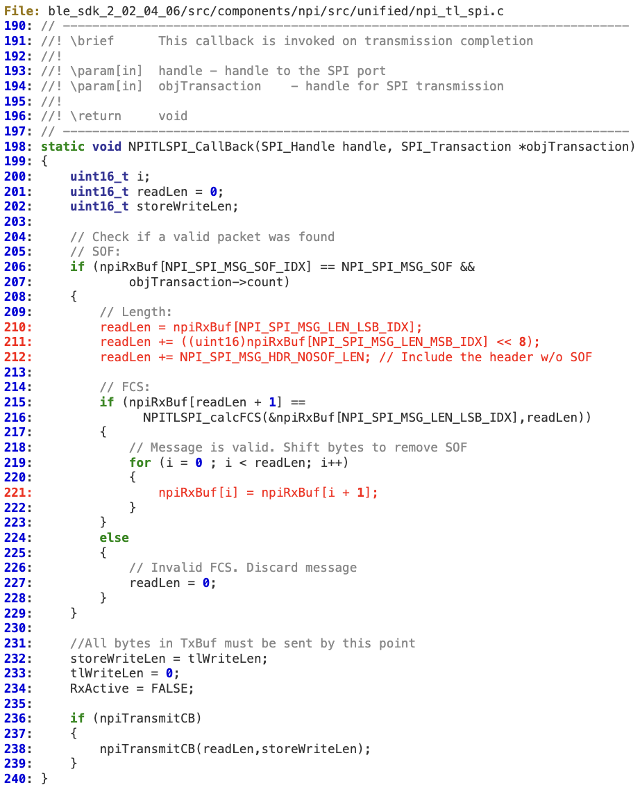
Memory corruption via ‘NPITLSPI_CallBack’
Affected Products
CC1350 SDK, BLE-STACK (SDK v4.10.01 and prior versions) CC26x0 BLE-STACK (v2.2.4 and prior versions)
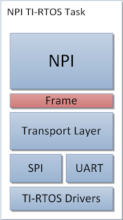
“TI’s Network Processor Interface (NPI) is used for establishing a serial data link between a TI SoC and external MCUs or PCs. It is an abstraction layer above the serial interface (UART or SPI) that handles sending / receiving data power management, and data parsing It is mainly used by TI’s network processor solutions.” Texas Instruments Website
Impact
A local attacker able to interfere with the physical SPI bus between the Host and NCP could send a malformed UNPI packet that corrupts dynamic memory in the Host, potentially achieving code execution.
Technical Details
When ‘NPITLSPI_CallBack’ parses the UNPI packet coming from the Slave, it does not properly verify whether the 16-bit length is within the bounds of ‘npiRxBuf’.
At lines 210-211, ‘readLen’ is directly calculated from the untrusted input coming from the slave.
Assuming that the local attacker will either guess or force a deterministic FCS by taking into account the malloc implementation, the memory corruption will take place at line 221.
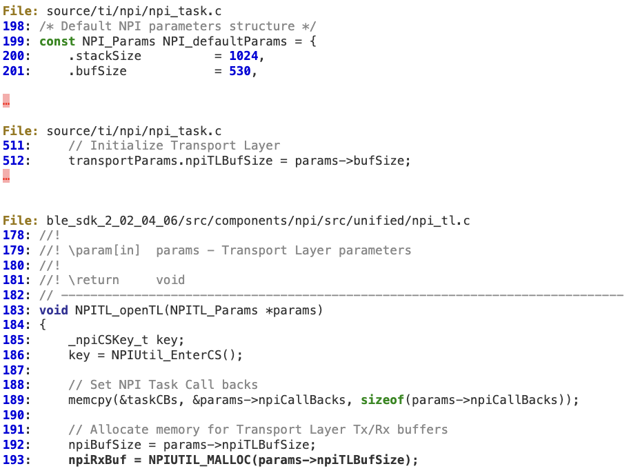
‘npiRxBuf’ is initialized at line 193, using the default value of 530 bytes.
Qualcomm – www.qualcomm.com
Vulnerability
Multiple buffer overflows when parsing malformed WMI packets in the ‘Wifi_qca’ middleware
“The Wireless Module Interface (WMI) is a communication protocol for QCA wireless components. It defines a set of commands that can be issued to the target firmware or that the target firmware can send back to the host for processing. This WMI communication is happening over the defined HIF layer.”
Impact
A local attacker able to interfere with the physical SPI bus between the Host and target QCA SoC could send a malformed WMI packet that corrupts kernel memory in the Host, thus potentially achieving local code execution with kernel privileges.
Technical Details
There are multiple places in the QCA middleware where WMI messages coming from the device are not properly validated.
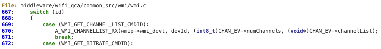
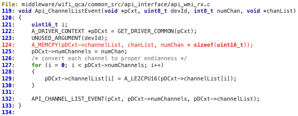
#1 ‘WMI_GET_CHANNEL_LIST_CMDID’
When processing ‘WMI_GET_CHANNEL_LIST_CMDID’ at ‘wmi_control_rx’ there is no sanity check for the attacker-controlled value ‘CHAN_EV->numChannels’.
‘Api_ChannelListEvent’ then uses ‘numChan’ to calculate the number of bytes, without performing any bounds checking, that will be copied into the fixed buffer ‘pDCxt->ChannelList’.
This buffer is defined within the Driver Context structure at line 256. In terms of exploitability, an attacker could easily overwrite a function pointer at line 272 with controlled values.
#2 ‘WMI_STORERECALL_STORE_EVENTID’
When processing ‘WMI_STORERECALL_STORE_EVENTID’ at ‘wmi_control_rx’, there is no sanity check for the ‘len’ value, in order to verify it is not larger than ‘pDCxt->tempStorageLength’. As a result, an overly large WMI packet could corrupt the fixed-length buffer pointed to by ‘strrclData’. This buffer is initialized at ‘Custom_Driver_ContextInit’.
This buffer is initialized at ‘Custom_Driver_ContextInit’.
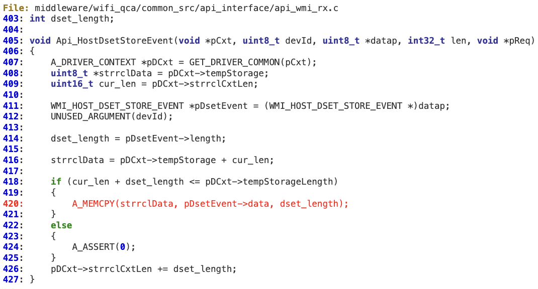
#3 ‘WMI_HOST_DSET_STORE_EVENTID’
At ‘Api_HostDsetStoreEvent’,’dset_length’ is an attacker-controlled value. At line 418, there is an integer overflow which could bypass the ‘if’ condition. As a result, ‘dset_length’ can still be larger than ‘pDCxt->tempStorageLength’, leading to memory corruption.
Any other code relying on ‘dset_length’ may also be vulnerable (e.g. ‘Api_HostDsetReadEvent’).
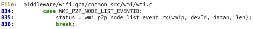
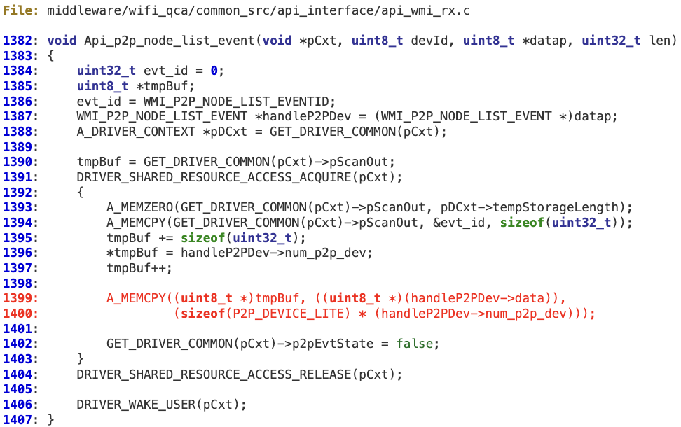
#4 ‘WMI_P2P_NODE_LIST_EVENTID’
When processing ‘WMI_P2P_NODE_LIST_EVENTID’ messages coming from the device, the attacker-controlled value ‘num_p2p_dev’ is not sanitized. As a result, at line 1399 it is possible to corrupt the fixed-length buffer pointed to by ‘tmpBuf’, which is ‘pCxt->pScanOut’ (actually, it is ‘pDCxt->tempStorage’, which has been previously explained).
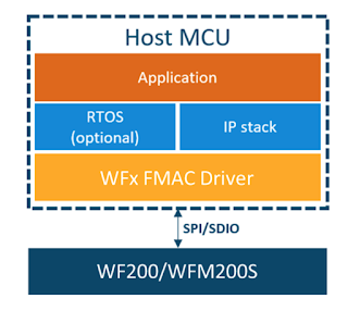
“The WFx FMAC driver is a software resource meant to allow a host to communicate with the WFx Wi-Fi transceiver. The API exposed by the driver gives control over the WFx Wi-Fi capabilities. In addition, the API enables data transfer at the IP level. This means that the host requires an IP stack if it wants to send/receive Ethernet frames.”
A local attacker able to interfere with the physical SPI/SDIO bus between the Host and the Silicon Labs NCP could forge a malformed WFx response frame that corrupts memory in the Host, thus potentially achieving local code execution.
Technical Details
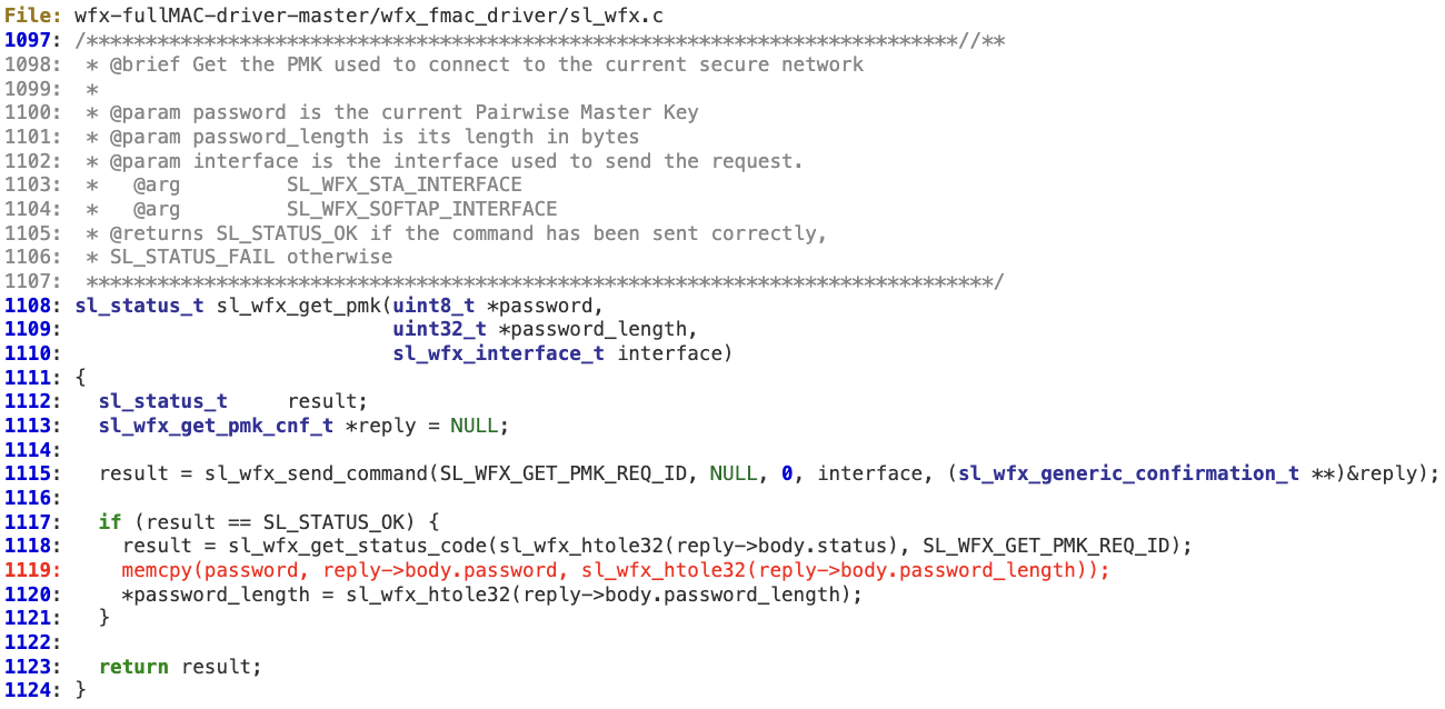
‘sl_wfx_get_pmk’ does not sanitize ‘reply->body.password_length’, by either comparing it to ‘password_length’ value or checking against SL_WFX_PASSWORD_SIZE, before copying it (line 1119) into the provided buffer. As a result, there is no guarantee that the buffer pointed by ‘password’ can safely receive the length specified in the response.
Vulnerability
Kernel memory corruption when decoding ‘Secure Channel’ HIF frame
Silicon Labs’ WF(M)200 chips have the ability to encrypt the SPI or SDIO serial link between the Host and the device.
Impact
A local attacker able to interfere with the physical SPI/SDIO bus between the Host and the Silicon Labs NCP could send a malformed HIF frame that corrupts kernel memory in the Host, thus potentially achieving local code execution with kernel privileges.
Technical Details
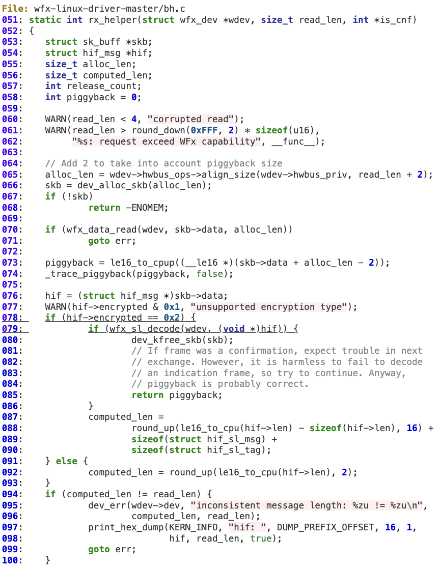
The driver handles attacker-controlled inputs (lines 78-80) when the HIF protocol is using the ‘secure channel functionality,’ even before the proper sanity check on the ‘hif->len’ field is performed (at line 94). As a result, the computed length for the HIF frame would be different from the actual ‘read_len’.
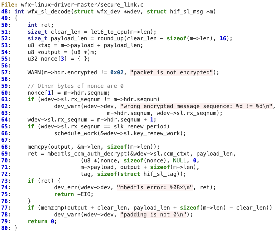
‘clear_len’ is controlled by the attacker, so ‘payload_len’, ‘tag’ and ‘output’ are also indirectly controlled to some extent (lines 51-54). At line 69, ‘mbedtls_ccm_auth_decrypt’ is invoked to decrypt the HIF payload using ‘payload_len’ with the ‘skb->data’ buffer as output. As the length of ‘skb->data’ may be different than ‘payload_len’, it is possible to corrupt that memory chunk.
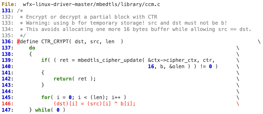
The actual memory corruption happens at line 146 in CTR_CRYPT as ‘dst’ is pointing to HIF’s payload.
Zephyr OS – www.zephyrproject.org
Vulnerability
Multiple buffer overflows in the ‘Zephyr’ eswifi driver
Affected Products
Zephyr RTOS 2.3.0:
– https://github.com/zephyrproject-rtos/zephyr
– https://www.zephyrproject.org/
Impact
A local attacker able to interfere with the physical SPI bus between the Host and target controller could send a malformed SPI response that corrupts kernel memory in the Host, thus potentially achieving local code execution with kernel privileges.
Technical Details
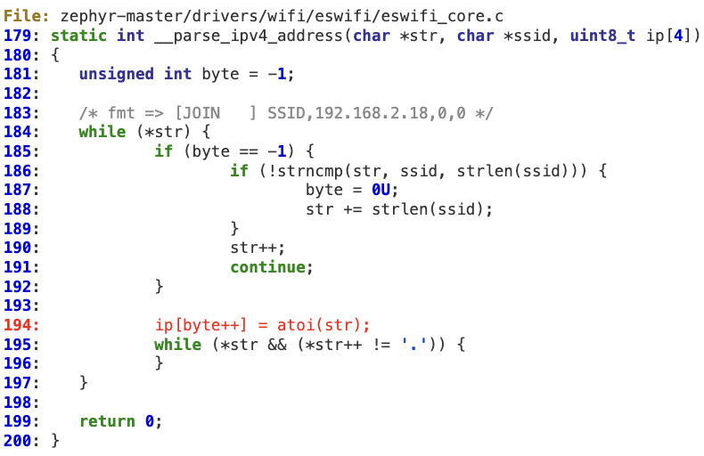
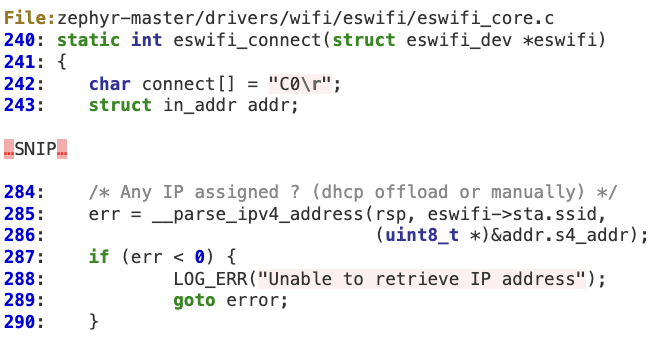
#1 ‘__parse_ipv4_address’ buffer overflow
This function does not properly verify that ‘byte’ is within IP’s bounds (4 bytes) when parsing the IPv4 address. As a result, a malformed IP string with an overly large number of ‘dots’ will corrupt the ‘ip’ buffer.
This vulnerability results in a stack overflow at lines 243 and 286.
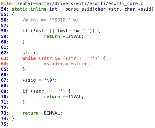
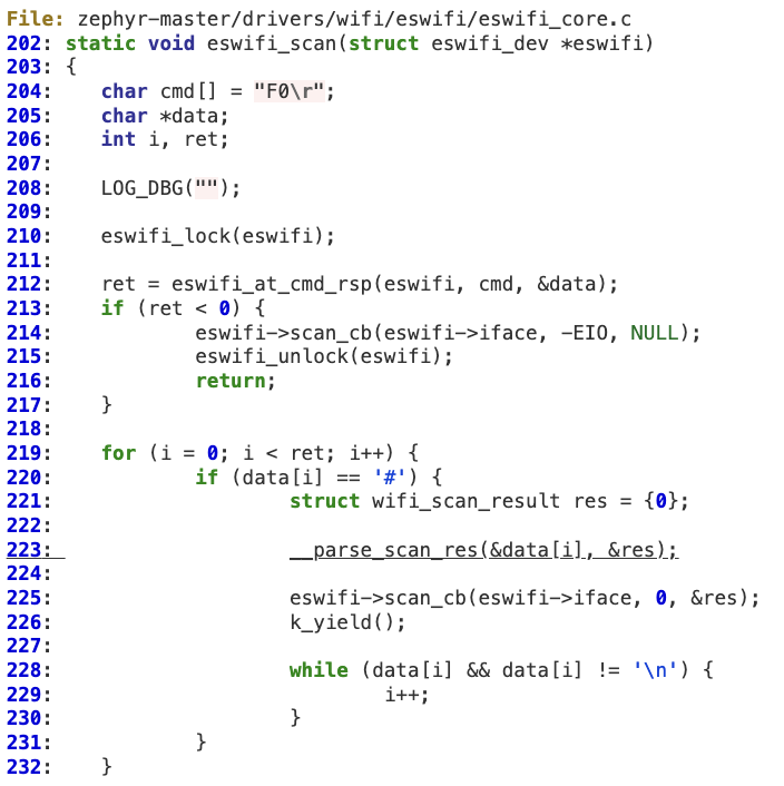
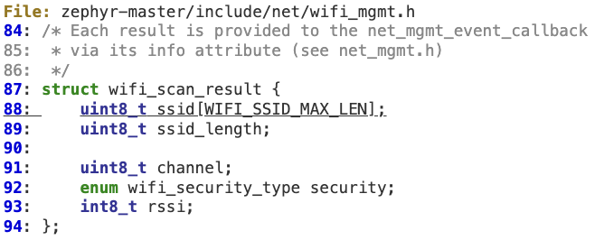
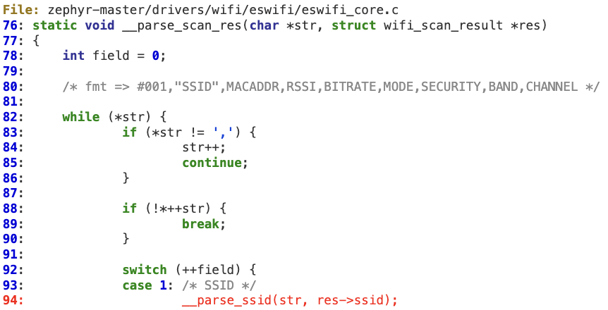
#2 ‘__parse_ssid’ buffer overflow
A similar situation can be found in ‘__parse_ssid’, which extracts and then copies the quoted SSID coming from the SPI response without checking its length.
This vulnerability also ends up in a stack overflow scenario according to the following vulnerable path:
1.
2.
3.
Microchip – www.microchip.com
Vulnerability
Multiple vulnerabilities in ‘CryptoAuth Lib’ 3.2.2
“Designed to work with CryptoAuthentication devices such as the ATECC608B, ATSHA204A or ATSHA206A and to simplify your development, the CryptoAuthLib is a software support library written in C code. It is a component of any application or device driver that requires crypto services from the CryptoAuthentication devices. It works on a variety of platforms including Arm® Cortex®-M based or PIC® microcontrollers, PCs running the Windows® operating system or an embedded Linux® platform“
Microchip Website
Impact
A local attacker able to partially emulate a malicious of Crypto Authentication device through USB could send malformed KIT protocol packets that corrupt memory in the Host, thus potentially achieving code execution.
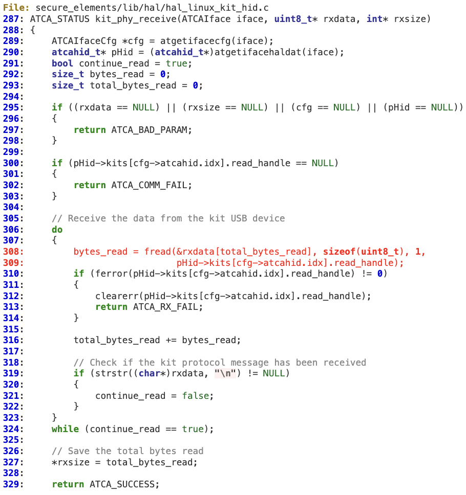
Technical Details
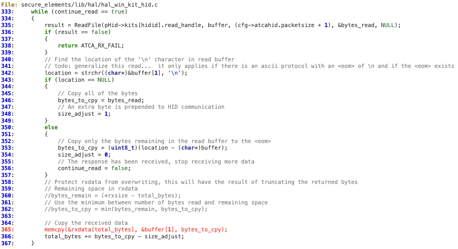
When ‘kit_phy_receive’ is receiving the KIT packet from the device, it does not properly verify whether the total amount of bytes received is within the bounds of ‘rxdata’.
The reading loop’s condition is merely ‘continue_read == true’ without taking into account ‘rxsize’, at line 324.
At line 308, we can see how the logic constantly tries to read a fixed amount of one byte from the USB device.
At line 316, ‘total_bytes_read’ is incremented by ‘bytes_read’. As the attacker controls the input, it is possible to evade the check for ‘\n’ at line 319. As a result, ‘total_bytes_read’ will be incremented beyond ‘rxsize’, thus overflowing ‘rxdata’ at line 308 during the call to ‘fread’.
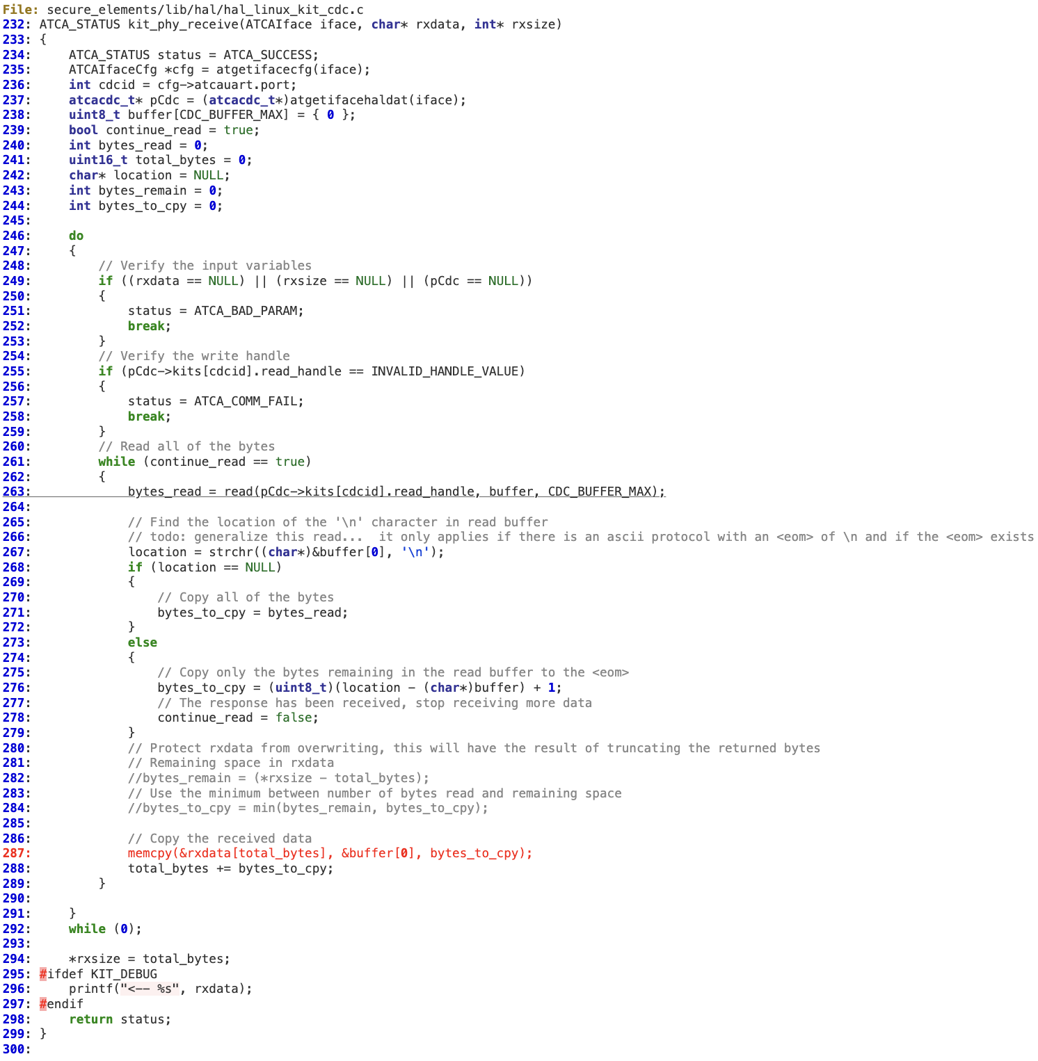
A similar issue can also be found in ‘kit_phy_receive’, although in this case instead of just one byte, it is reading CDC_BUFFER_MAX to a local stack buffer at line 263. ‘bytes_to_cpy’ is used to increment the offset (‘total_bytes’) (line 288) where the bytes will be copied (line 287).
A similar situation is found below, where the function is constantly trying to read ‘cfg->atcahid.packetsize + 1)’ and then copy to ‘rxdata’ at lines 365 without performing any bounds checking.
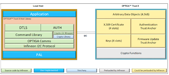
Infineon – www.infineon.com
Vulnerability
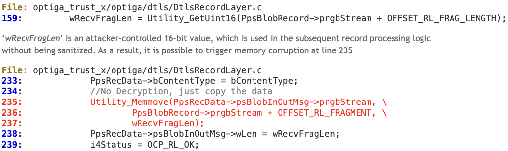
Memory corruption via ‘DtlsRL_Record_ProcessRecord’
A local attacker able to interfere with the physical I2C bus between the Host and Optiga Trust X security chip could send a malformed DTLS record that corrupts heap memory in the Host, thus potentially achieving local code execution.
Technical Details
During the DTLS handshake, the fragment length field of a DTLS record is not properly sanitized.
‘PpsRecData->psBlobInOutMsg->prgbStream’ points to a dynamically allocated buffer whose size is fixed (TLBUFFER_SIZE 1500 bytes).
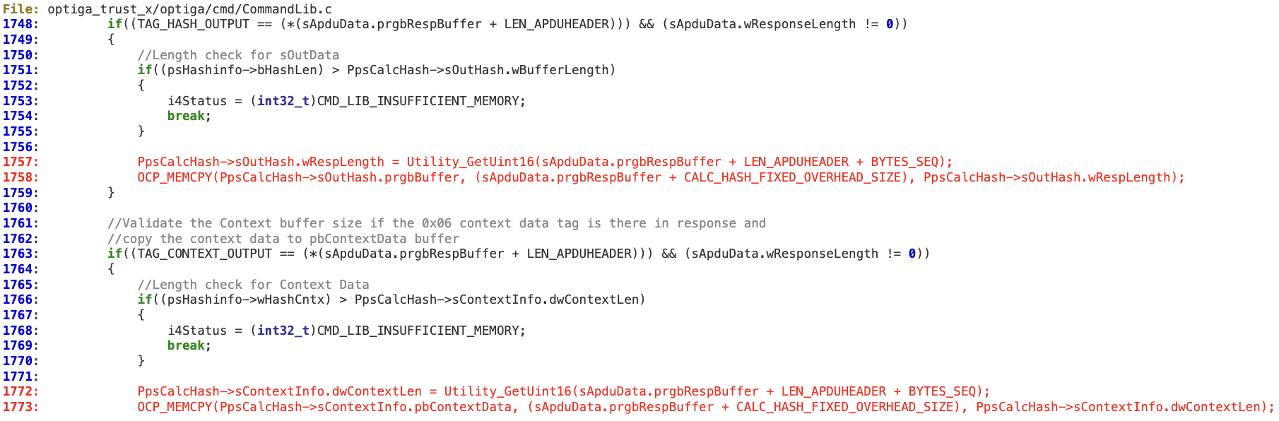
A local attacker able to interfere with the physical I2C bus between the Host and Optiga Trust X security chip could send a malformed ‘CmdLib_CalcHash’ response that corrupts memory in the Host, thus potentially achieving local code execution.
Technical Details
In the ‘CmdLib_CalcHash’ function, a potentially untrusted length field is used without being sanitized.
The tag length is directly obtained from the response buffer at line 1757, which could contain a value larger than ‘PpsCalcHash->sOutHash.wBufferLength’.Then at line 1758, this length is used to perform a ‘memcpy’ operation that will trigger the memory corruption. The same issue applies to lines 1772 and 1773.
Vulnerability
Multiple memory corruption issues in ‘Optiga_cmd.c’
A local attacker able to interfere with the physical I2C bus between the Host and Optiga Trust M security chip could send a malformed response that corrupts memory in the Host, thus potentially achieving local code execution.
Technical Details
In the ‘optiga_cmd_gen_keypair_handler’ function, a potentially untrusted length field is used without being sanitized.
The private key tag length is directly obtained from the response buffer at line 2576, which could contain a value larger than the buffer pointed by ‘p_optiga_ecc_gen_keypair->private_key’. Then at line 2579, this length is used to perform a ‘memcpy’ operation that will trigger the memory corruption.
The same issue applies to lines 3068 and 3072 while processing the ‘Calc_Hash’ response in function ‘optiga_cmd_calc_hash_handler’.
INSIGHTS, RESEARCH | January 28, 2021
Probing and Signal Integrity Fundamentals for the Hardware Hacker
By
Andrew Zonenberg
The latest new widget just showed up on your desk. You excitedly crack open the case, look around a bit, and find a signal that looks interesting. You fire up your oscilloscope, touch a probe to the signal, and… the widget won’t boot! Or maybe it works fine, but you see garbage on the scope screen that looks nothing like a useful digital waveform.
It’s a problem that’s becoming all too familiar to hardware hackers. As technology advances, signals become faster, which makes them more sensitive and less tolerant to the sloppy wiring and probing techniques commonly used in reverse engineering. Even cheap SPI flash can run at 100+ MHz in modern designs.
This article will focus on practical problems and solutions for analyzing existing boards, without digging too deep into the more advanced electrical engineering theory needed for design of high speed logic. For a more in-depth treatment of the subject, High Speed Digital Design: A Handbook of Black Magic (1993) by Howard Johnson & Martin Graham is an excellent read, as well as its successor High Speed Signal Propagation: Advanced Black Magic (2003).
If your probing setups look like this, you’re going to have a bad time reversing modern hardware!
At this level, the main thing to be aware of is that electrical signals move through wires at a finite speed, typically around 0.6-0.7x the speed of light (roughly six inches per nanosecond), and that changing cable characteristics (more specifically, impedance) causes an impact on the signal whose duration in time is proportional to their length.
Before we proceed any further I’d also like to introduce an abbreviation from the test equipment world that you may not be familiar with: DUT (Device Under Test). This is a fancy way of saying “the thing you’re trying to probe”.
Avoid Long Messes of Wires
In the photo above, a JTAG adapter was connected to the DUT with several feet of wire, without paying any attention to impedance or termination. The JTAG software was unable to detect the processor. When an oscilloscope was connected to the TCK signal on the DUT, the signal looked like this:
JTAG TCK signal with long wires
The rising edge of the clock signal climbs for a while, then dips, then continues climbing to its full value. These non-monotonic edges are a big problem! If the position of the dip happens to line up with the threshold of the device’s input pin, it will see two rising edges instead of one, resulting in a bit of data being duplicated.
You might be tempted to reduce the clock frequency of the JTAG adapter in this case, but this won’t help: all it will do is move the rising and falling edges further apart without changing their shape. Fast edges at 1 kHz are just as vulnerable as edges at many MHz.
Adding filtering to slow down the edge rate (at the cost of reducing the max operating speed), adding a ~33Ω series terminating resistor at the source end of the wire, or playing with ground geometry to match the impedance of the cable more precisely can all help. In most cases, however, the easiest solution is simply to shorten the wires.
No more spaghetti!
JTAG signal with shorter wires
If you look closely a small defect on the edge is still visible since the ribbon cable isn’t impedance matched, but it’s much smaller because the mismatched cable length is shorter. At this edge rate, this sort of defect shouldn’t be a problem since it doesn’t dip, it just stops rising momentarily. When dealing with sharper edges, you might want to shorten the cable even further. You should also…
Properly Secure Wires
This isn’t strictly a signal integrity issue, but “my wires ripped off the DUT” will certainly lead to difficulty seeing the intended signal! Properly securing wires and probes is something overlooked far too often.
Don’t rely on solder joints to provide mechanical support for a cable, which can be subject to bending and pulling forces as the DUT and cable move around your bench. If you’re lucky the solder joint will fail and the probe will cleanly separate from the DUT. Worse yet, you might rip the copper pads/traces off the DUT or ruin your probe.
There are plenty of different methods of securing wires, so pick one that suits your specific scenario. I prefer to secure the wire first, then solder it, in order to keep it from flailing around while I’m soldering.
Hot glue: Cheap and easy, but hard to do neatly and difficult to rework if you get it somewhere you didn’t intend. Requires rapid work to get things positioned right before it hardens and leaves annoying “strings” everywhere.
Kapton tape: Easily removable, but fairly low holding strength. You can buy it on big spools but I prefer using pre-cut dots to save lab time. Name-brand tapes generally have much better adhesive than cheap knockoffs.
Kapton tape securing a solder-in probe tip
Epoxy: Very strong, but almost impossible to remove once cured. Good choice for permanently attaching to something you plan to keep around the lab for an extended period of time.
UV cured wire tacking glue: My personal favorite (I’m a fan of Dymax #9-911, but there’s many other options). It cleans up easily with alcohol in the uncured state, and solidifies in a minute or two under a cheap gel nail polish curing lamp. Most of these glues have intermediate holding strength: the wire is unlikely to come free by accident, but careful prying with a knife blade will cleanly separate it from the DUT without damage.
Wires secured with UV glue
Probe holders: There’s a wide range of these available, ranging from DIY 3D printed bipods to $500+ three-axis micrometer jigs. More temporary in nature than any kind of adhesive, but useful for any time you want to look at more than a handful of signals while keeping your hands free. These get the probe tip right up against the board without any additional wire, which is great for probing faster signals.
Probe held in a bipod positioner
Avoid Long Probe Grounds
Yes,I’m talking about that big “tail” on your scope probe with an alligator clip at the end. Forget about using it on anything fast. It’s very inductive, which when combined with the capacitance of a typical passive probe creates resonances.
10 MHz clock seen through a 10MΩ probe with a long ground wire
In the 10 MHz clock seen above, the ringing isn’t enough to completely destroy the shape of the signal, but it doesn’t take much imagination to see that with anything a little bit faster, the signal would be completely unreadable.
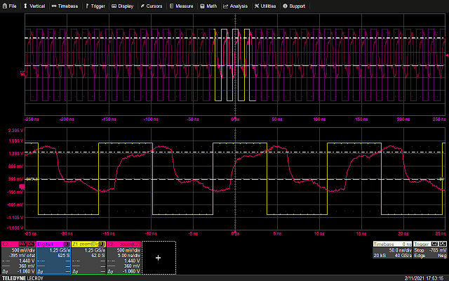
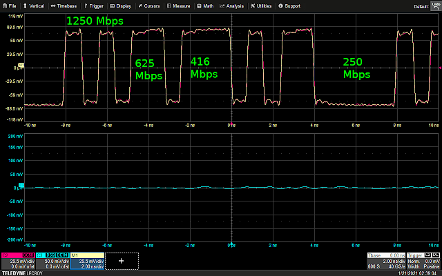
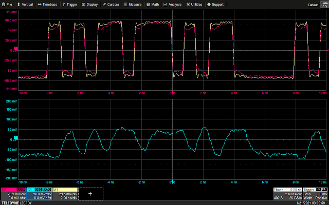
In the next few examples, we’ll be looking at a 1.25 Gbps Ethernet signal. The “idle” sequence between packets contains a nice mix of fast 0-1-0-1 transitions and runs of several 0 or 1 bits, providing a nice idea of what a data bit at different rates might look like through a given probing setup.
Test signal with no probe
In this screenshot we see three different signals:
Blue: The signal as seen through the probe (flatlined, since the probe isn’t on the board yet).
Pink: The signal internal to the DUT
Yellow: A snapshot of the pink waveform frozen in time. Right now they’re identical, but if the probe alters behavior of the DUT you’ll see them deviate.
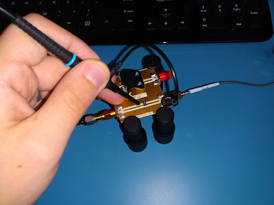
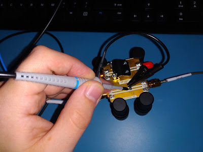
To start, let’s use a standard 10MΩ passive scope probe (a Teledyne LeCroy PP022) and an alligator clip ground.
Probing the easy, obvious way.
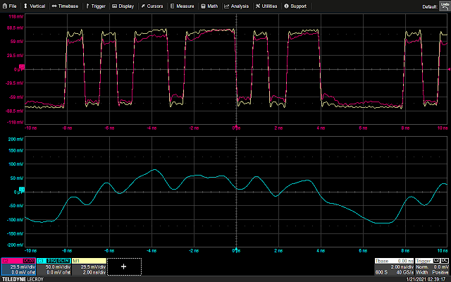
And here’s what the scope sees
The signal is completely unrecognizable through the probe! In addition to causing ringing on edges, the inductance of the long ground lead destroys high frequency performance.
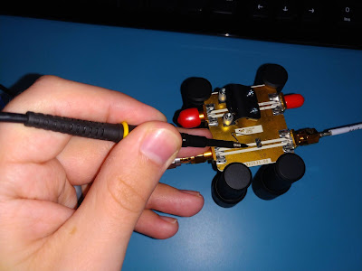
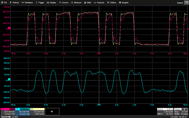
A spring ground is a bit trickier to use since you have to find a good ground point fairly close to the signal you’re probing on the DUT, but gives a much nicer looking view of the signal.
Using a spring ground
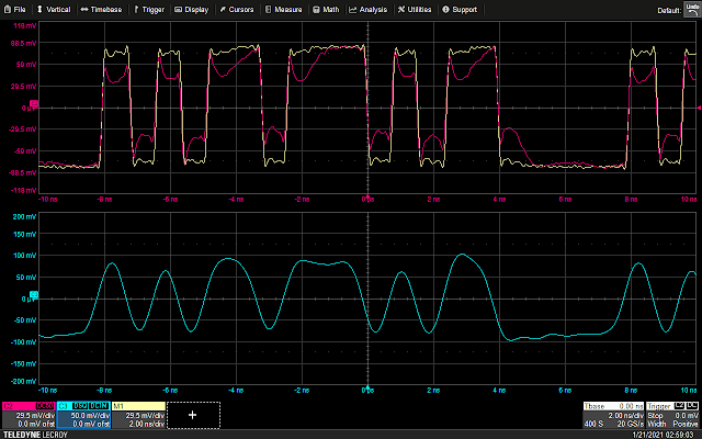
Waveform seen with the spring ground
That’s a lot better looking: the edges are rounded off and not as square looking as they should be, but that’s an inherent limitation of this probe (500 MHz bandwidth). Individual data bits are clearly readable, so all is well… right?
Wrong. Take a look at the signal on the DUT (pink waveform)! There’s huge dips in it. This might well be enough to corrupt data and render the DUT nonfunctional. This brings us to our next topic…
Beware of Probe Loading
You might be inclined to look at the “10MΩ” marking on a scope probe and assume that it imposes infinitesimal load on the DUT. That may be true at DC, but not at frequencies typical of modern electronics.
The problem is that typical 10MΩ scope probes also have on the order of 10 pF of capacitance. When a high frequency signal is applied to a capacitor it acts somewhat like a resistor, with an effective resistance of 1/(2*pi*f*C) for frequency of f Hz and capacitance of C farads. So the actual load the probe imposes is around 159Ω at 100 MHz and 31Ω at 500 MHz – a far cry from the 10MΩ seen by a DC signal! Since this loading is frequency dependent it will distort the signal as well as weakening it, potentially rendering it unreadable to the intended destination on the DUT.
Unfortunately, there’s no trivial way to work around this issue using a standard passive scope probe, but there are several different types of probe designed for higher speed use which can help.
Active probes, which contain an amplifier in the probe head, can have much lower capacitive loading. A typical 1.5 GHz active probe might have an input capacitance of 0.9 pF, making it much less invasive. The price you pay for this is very expensive hardware – active probe price tags start in the low four figures (USD) and go up from there.
For looking at typical digital signals, a good low-cost option is the transmission line probe. This has a low-value resistor, typically 450Ω, at the tip and connects via coaxial cable to an oscilloscope input terminated with a 50Ω resistor to ground, for a total of 500Ω of loading as seen by the DUT. (Although this may present a problem when looking at signals with pull-up resistors, these are typically low enough speeds that a conventional 10MΩ probe can be used instead.)
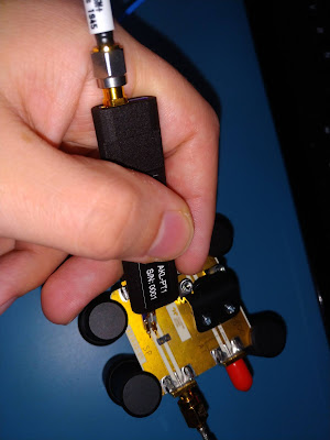
Probing our test setup using a transmission line probe (Pico TA061)
Waveform seen through the transmission line probe
The benefit of a transmission line probe is that the input load is, in theory, purely resistive. Although there’s always trace amounts of “parasitic” capacitance due to the physics of having the ground a finite distance away from the input, it’s normally a fraction of a picofarad, which results in a high speed signal on the DUT being loaded much less heavily. As if that wasn’t good enough this lower capacitance means that a high-inductance ground, like the standard alligator clip lead, will be much less likely to resonate – allowing this poor quality (but convenient) grounding method to be used with much faster signals.
In this screenshot the signal is clearly intelligible despite the long ground, and while the waveform as seen by the DUT has measurable loading it’s far less severe than with the 10MΩ probe.
Waveform seen through transmission line probe with spring ground
Unsurprisingly, switching the transmission line probe to a spring ground improves the signal quality further – however, some degradation of the signal on the DUT is also visible. This is caused by the ~2 pF of parasitic capacitance of the probe. (The higher inductance ground lead concealed this loading in the previous test.)
If you don’t want to spend $329 for a commercially made entry level transmission line probe (or $1K+ for a higher end transmission line probe like the Teledyne LeCroy PP066 or PicoConnect 900 series), you may wish to consider building your own. Simply solder a 450Ω resistor to the signal on the DUT you wish to probe, then solder the center terminal of a piece of 50Ω coax to the other end of the resistor and solder the ground braid to any convenient ground point nearby on the DUT. Attach the other end of the coax to your scope and you’re in business.
Squeezing maximum performance out of this DIY probe design requires careful engineering, but building something that outperforms a standard 10MΩ passive probe for instrumenting fast digital logic isn’t difficult. If you don’t want to spend the time tweaking it, you might also want to consider…
Open Hardware High-Speed Probes
For the past year or two I’ve been working on two open-hardware transmission line probes, the AKL-PT1 (handheld, 6 GHz bandwidth) and AKL-PT2 (solder-in, 4 GHz bandwidth).
These probes target the OSHPark 4-layer and flex board stackups respectively. They’re still being fine tuned but already deliver very nice results (outperforming every <$2K probe I’ve tested them against) so feel free to download the KiCAD files and try building one!
There will probably also be a group buy of assembled units with nice plastic enclosures and proper impedance control at some point in the near future once I’m finally satisfied with their performance.
AKL-PT1 in use
AKL-PT2 soldered to a board
Same Ethernet test signal seen through the AKL-PT1
With this knowledge, you should be able to acquire more accurate and useful data from your embedded targets.
INSIGHTS, RESEARCH | January 7, 2021
TAPing the Stack for Fun and Profit: Shelling Embedded Linux Devices via JTAG
By
Ethan Shackelford
While it may not come as a surprise to those who have worked with embedded devices, it is not uncommon to find the JTAG interface on embedded devices still enabled, even in production. Often cited as providing “ultimate control” over a device, JTAG debugging usually provides the user with full read/write privileges over device memory (and by extension over MMIO) as well as the ability to read and write control registers.
On a simpler embedded device (for example, a “smart” lock), leveraging open JTAG can be fairly straightforward: dump the bare metal firmware via JTAG, reverse engineer it to determine the details of its operation (such as the function which performs validation on the entered PIN code), and either use the JTAG interface to re-write the firmware in flash, or flip some bits in memory (in this example, to trick the PIN code check logic into accepting an invalid PIN code).
However, embedded Linux platforms can complicate this process substantially. First, the firmware is not bare-metal, but instead a complex system including a multi-stage bootloader, the Linux kernel image, and various filesystems. Second, storage devices are more likely to be managed and mounted by the kernel, rather than memory-mapped, making access to peripherals over JTAG substantially more complicated than on bare metal systems. Third, MCUs used for embedded Linux tend to have a more robust MMU and memory management scheme, which can make addresses reported by the MMU during JTAG memory access more difficult to correlate to locations in physical memory — a correlation that is sometimes necessary thanks to the second hurdle created by a more robust MMU, where it also restricts memory access depending on the execution context, which means that the MMU must either be disabled entirely, or configured to suit the task at hand.
Thus, while open JTAG does usually grant ultimate control over a device, the operations performed are sufficiently low-level as to make actually manipulating a Linux system in this way a difficult and somewhat arcane task. However, operating in a Linux environment does have its perks: rather than the more complex task of manipulating device operation directly over JTAG in a way specific to the particular device being tested as is the case for bare-metal operating systems, leveraging JTAG on any Linux-based device typically revolves around a uniform goal: access to a root shell. This uniformity means that a similar group of techniques can be used to gain access in any case where a Linux-based device has an enabled JTAG interface.
Despite the obvious and widespread nature of this issue, there appears to be little to no existing work published on this topic. To help fill this void, this article is intended to detail the process of using access to a JTAG interface to move to a root shell on a Linux-based device, as well as the common issues and pitfalls which may be encountered therein.
Interacting with the TAP controller
While this document will not go into great detail on the inner workings of JTAG and the associated tooling, the following is a short crash course on using OpenOCD and a JTAG hardware adapter to interact with a device’s TAP controller.
Interacting with a device via JTAG requires some means of driving each its pins. This can be accomplished with specialized hardware, such as the SEGGER J-Link series of adapters (which I will use for the purposes of this article), or just as easily with a more generic device like a Bus Blaster or FTDI dongle, such as an FT2232. The experience with a device will vary depending on how well it is supported by OpenOCD — the Bus Blaster and SEGGER J-Link are both well supported.
Determining JTAG pinout on a given board is outside of the scope of this document, but a wealth of information for doing so exists online. Once the pinout has been determined, the device under test and the chosen JTAG adapter should be connected appropriately. Pictured below is the example device and a J-Link adapter, connected based on the determined pinout of the board’s JTAG header.
After connecting to the device, OpenOCD can be used to interact with the TAP controller. In order to do so, OpenOCD requires information on the CPU to which you’re connected and the adapter used for the connection. A standard installation of OpenOCD will include configuration files for a number of common adapters and targets. It supports many adapter/target combinations out of the box, and on a standard installation the appropriate configs can be found in the target, board, and adapter subdirectories of /usr/local/share/openocd/scripts.
In this example, we’re working with an NXP iMX.28 CPU, and the SEGGER J-Link, so the call to OpenOCD looks like the following:
To verify a valid connection, confirm that the reported IDCODE (here 0x079264f3) matches the expected value for the targeted processor; this information can be found in the datasheet for the processor.
For simple, manual interaction, OpenOCD exposes a telnet listener on port 4444. OpenOCD can also be loaded with TCL script files at launch, by passing additional “-f” flags pointing to the desired scripts.
Now that we can talk to the TAP controller, we can move on to the various techniques for leveraging the JTAG interface.
Techniques
Depending on the processor, the actual implementation of various functions available over JTAG may differ. In general, the same set of primitives will be available: read/write to flash and other memory mapped IO, read/write to various CPU-specific control registers, and read/write to RAM. If you’re familiar with more traditional exploitation techniques, these probably sound a lot like read-where/write-where memory-corruption-based exploitation primitives; this is a useful way of thinking of them.
There are a few constraints to keep in mind while attempting to gain code execution on a Linux device over JTAG:
While the JTAG interface has full control of the processor, this doesn’t mean that extra steps won’t be required to make use of it. For example, the debug interface write to any area of RAM, but it will be doing so in the same context as whatever program was running when the CPU was halted. In the context of a Linux system, this means the same rules that apply to programs apply to any memory access by the debug interface – access an area of memory outside the virtual memory space of the currently executing process, and the MMU will reject the memory access and generate a DATA ABORT exception.
Not all execution contexts are created equal. Anyone taking their first steps toward exploiting Linux kernel modules will know that code executed from the context of the kernel (or “Supervisor” from the perspective of the CPU) is generally incompatible with code and exploitation techniques written for userland. While it is possible to tailor shellcode to either context, the context should be kept in mind when setting things up.
As we will see shortly, making our way to a shell from these primitives involves overwriting some section of memory. Of course, if the code or data we overwrite with shellcode is critical to system operation in some way, the system will no longer function as expected, so take care in selecting an area of memory that can be overwritten without interfering with the system as a whole.
For these examples, the following conditions were chosen for exploitation:
We will be exploiting the JTAG access from userspace, rather than from kernel code. There is no real reason for this, other than the fact that it’s a bit simpler than acting from kernelspace, and it so happens that any shell on the device under test will be a root shell, so we don’t gain any additional privileges by going the kernelspace route.
The device under test provides an Ethernet interface for communication with the outside world. This will be our target for gaining a shell by opening a reverse shell over an unused TCP port. If the device did not have this interface and instead had, say, a UART console, the timing, memory areas, and shellcode chosen would differ somewhat. However, the overall procedure in this article would still apply.
The first step is simply to generate some valid shellcode to load into memory. To generate shellcode for performing our chosen operation, a reverse TCP shell, we use MSFvenom, specifying the target architecture/platform (armv5le, linux). We want the raw byte output, as we’ll be injecting it directly into memory.
As illustrated above, the size of the shellcode in this case is 172 bytes. Not huge, but it could certainly pose a problem depending on how the MMU is configured. In fact, in the case of our example device, this tends to exceed the MMU-allowed writable length of memory under $pc, and we will need to address it as we perform some of the techniques outlined below.
Smashing with Precision
Although the famous Phrack article is nearly a quarter-century old at time of writing, the old-school stack smashing of days gone by is alive and well in the embedded world. It is not an entirely uncommon, depending on the architecture family/version and degree of programmer negligence, to find devices in the embedded world which either do not have a “no execute” flag for memory access, or have the flag disabled if it is available. If this is the case, gaining a shell is very straightforward: halt the CPU, overwrite the stack with shellcode, and jump to $sp. In most cases, the stack will have enough space allocated to avoid generating a segmentation fault on write, and is always writable by nature, enabling us to sidestep any MMU shenanigans that might be required for other techniques during exploitation.
This technique requires little to no knowledge of the software running on the device, and generally will not crash or permanently alter the operation of the device. It still might crash, if you get unlucky with the function whose stack is being overwritten, and so isn’t suitable for testing environments where any degree of device malfunction is unacceptable.
A number of factors may exclude this technique as a possibility, such as a no-execute bit or stack constraints. It may be possible to work around these factors via the JTAG interface, but in the case that a workaround fails, other techniques are available.
Firing From the Hip
In general, device exploitation can be aided by access to a copy of the firmware. If firmware is not available, it’s possible to feel your way around the system semi-blind, halting and inspecting configuration registers to determine when you’ve landed in a suitable place. This technique will also routinely crash the device, unless you get incredibly lucky on your first attempt, so this is not a technique suited to an environment where a crashed device is not a recoverable scenario.
The MMU will need to be addressed to allow manipulation of memory, so that shellcode can be written and execution resumed without generating a fault. To do so, we can either reconfigure the MMU to allow reads/writes to the areas to which we want to write, or just disable the MMU entirely. The former option is more complicated to set up, but the latter requires extra work since without the MMU we’ll need to translate virtual addresses to physical addresses ourselves. However, disabling the MMU is also a more universal option, easily applied to a variety of CPUs and architectures.
Here we opt for disabling the MMU, writing shellcode under the memory pointed to by the program counter, then re-enabling the MMU to allow execution to continue without error. There are a few techniques for correlating MMU-enabled (virtual) addresses with the MMU-disabled (physical) addresses; in this case, dumping the full system RAM via JTAG with the MMU disabled, then using a simple homemade tool to match the bytes under the program counter to an offset into the RAM dump.
This tool can be used with the output of OpenOCD’s dump_image command to find where, in the physical address space, a given virtual address is pointing. While the dumped RAM image may not be identical between boots, the locations of loaded binaries in memory will generally stay the same, because the device will tend to run the same programs in the same order every time.
The image above illustrates the process of using OpenOCD in conjunction with the tool:
The CPU is halted here, and found to be in the “User” execution context. If it had been halted under any other context, most likely “Supervisor,” the CPU would be resumed, and the process repeated, until the CPU is halted in the correct execution context. 1024 bytes starting at the program counter are then dumped to a file.
That resulting file is fed into the tool, and found within the dumped RAM image. The tool outputs the address at which a matching sequence of 1024 bytes is found (the physical address).
The MMU is disabled here, and the shellcode is written to the physical address to which the virtual address in the program counter is mapped. The process of disabling the MMU is CPU-specific; information on how to do so can be found in the appropriate reference manual. Here it is accomplished by clearing a specific bit in a specific control register.
The MMU is re-enabled and the memory under the program counter is read to confirm the shellcode has been written. The bytes read match the bytes of the shellcode, confirming we have written to the correct physical address.
The CPU is resumed, with execution continuing from the program counter, our shellcode now occupying the memory to which it points. The netcat listener receives a connection, and a bash shell is available to the attacker. In this case, the shell runs with root privleges.
So, easy right? Not exactly.
The far more likely outcome during the above process is that the userspace code we randomly halted on will either be some crucial library function, causing a crash at some subsequent step in execution of the shellcode, resulting in a failure to gain a shell and probably breakage of most other device functionality (think overwriting malloc with shellcode), or some piece of code whose absence prevents successful shell access. In practice, actually getting through this process with a shell at the end required around 20-30 attempts on average, with many failed attempts requiring a device reset to un-break critical library code.
This is fine, if tedious, under circumstances where a device can be reset and taken down arbitrarily. However, in contexts where a device cannot be taken offline or reset, this approach is obviously not viable.
Know Thine Enemy
In cases where device firmware is available, or where the exact version of libraries or other software in use by the system are known or possessed, we can take a more targeted approach. The ability to identify the location in physical memory of a binary or library known to be called during device operation enables us to overwrite a function from within that binary or library with shellcode. Upon execution of that particular function as part of the normal operation of the device, the shellcode will run in place of the function normally at that offset into the binary. When we can choose a function to overwrite whose abscence will not cause any anacceptable side effects for the device, we can avoid device crashes or other interruptions.
In the case of the example device, the firmware is available, and we can use one of a variety of binary analysis tools to determine an appropriate function to overwrite. IDA, Binary Ninja, radare, and even the humble objdump are just fine for this purpose. For this example we’ll use Binary Ninja.
In looking for an appropriate function, we should seek the following conditions:
The binary or library should be loaded at startup, and continue running during device operation. This ensures that it will be present in RAM when memory is dumped, and that its position in RAM will be the same between boots. This rules out something like a cgi-bin called in response to an HTTP request, which would otherwise be a good candidate.
The function should either have some external attacker-accessible trigger, or should be a function that repeats reliably. If the function only runs once, during system boot, the shellcode will never actually execute if it’s loaded after the function has been executed.
The function should not be system-critical, especially in the case of standard libraries. Its fairly trivial to track down an appropriate version of libc or libpthread, for example, and simply overwrite something like pthread_mutex_unlock, with a pretty strong guarantee that the function will run at some point, triggering the shellcode. However, the next time a function needs to unlock a mytex, the system will come crashing down, requiring a reset.
While not required, it can be useful to choose some binary or library whose source code is publicly available, as the code can come in handy to work out the most appropriate function to overwrite and save some time otherwise spent reverse engineering.
After some digging around, we identified a good candidate for shellcode injection in a vsftpd server running on the device. Exclusively used for OTA firmware updates, a lapse in functionality in this server will not interfere with the operation of the device. In a real-world scenario where the ability to initiate an OTA update would eventually be required again, after acquiring root shell access the vsftpd server can be restarted and reloaded into memory uncorrupted by shellcode.
Some minimal reverse engineering and cross-referencing against the vsftpd source turns up a function, vsf_sysutil_retval_is_error, which looks like a good choice. It appears to be vsftpd’s error checking function, meaning it will likely be called during most operations. This is supported by a fairly large number of cross references in a wide range of functions. One drawback is that the function itself is only eight bytes long, and overwriting it will clobber the function positioned under it in memory. This means that the vsftpd server is toast after our exploit is fired, but as mentioned before, we can simply restart the vsftpd server from our root shell if desired.
Using the same tool as in the previous techniques, we find the physical address in RAM of the function we’d like to overwrite. This time, rather than searching for the bytes dumped from under $pc, we look for 0x100 bytes or so from the vsftpd binary, starting at the beginning of the target function. This can be done with dd, or just by copying-and-pasting if you’re using Binary Ninja or similarly equipped software.
Moving back to the JTAG connection, we can now write to the acquired physical address (shown in the preceeding image), overwriting the target function with shellcode. To trigger its execution, we’ll use an FTP client to connect to the target device, which at some point calls the vsf_sysutil_retval_is_error function as expected.
Further Reading
JTAGTest.com Pinout Reference – A useful collection of various standard JTAG header pinouts, useful for identifying mystery pinouts on boards under test.
Smashing The Stack For Fun And Profit – A must read for the aspiring hardware hacker, many of the points discussed within apply equally when working with a device over a JTAG connection.